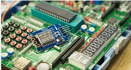
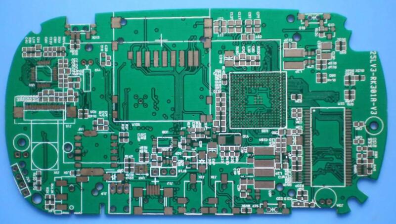
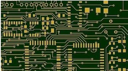
PCB design is very important in the entire PCB board, it determines the basis of the entire circuit board. The editor summarizes some important points that need to be paid attention to in PCB design for reference.
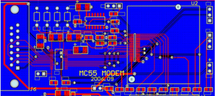
1. Choose PCB board
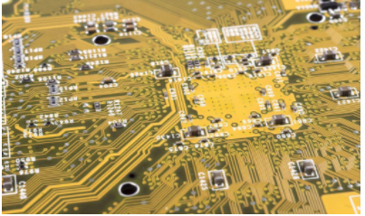
The choice of PCB board must strike a balance between meeting design requirements and mass production and cost. The design requirements include both electrical and mechanical parts. This material issue is usually more important when designing very high-speed PCB boards(frequency greater than GHz). For example, the commonly used FR-4 material, the dielectric loss at a frequency of several GHz will have a great influence on the signal attenuation, and may not be suitable. As far as electricity is concerned, pay attention to whether the dielectric constant and dielectric loss are suitable for the designed frequency.
2. Avoid high frequency interference
The basic idea to avoid high-frequency interference is to minimize the electromagnetic field interference of high-frequency signals, which is called crosstalk (Crosstalk). You can increase the distance between the high-speed signal and the analog signal, or add ground guard/shunt traces next to the analog signal, but also pay attention to the noise interference of the digital ground to the analog ground.

3. Solve the problem of signal integrity
Signal integrity is basically a problem of impedance matching. The factors that affect impedance matching include the structure and output impedance of the signal source, the characteristic impedance of the trace, the characteristics of the load end, and the topology of the trace. The solution is to rely on the topology of termination and adjustment of the wiring.
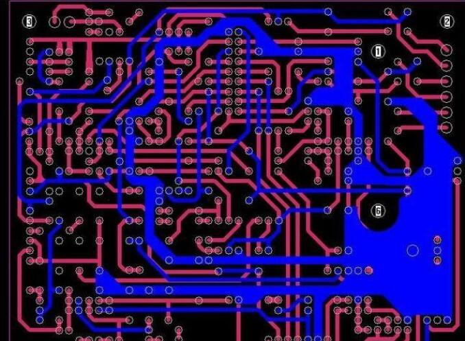
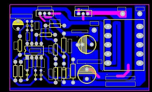
4. Realize differential wiring method
There are two points to pay attention to in the layout of the differential pair. One is that the length of the two wires should be as long as possible, and the other is that the distance between the two wires (the distance is determined by the differential impedance) must be kept constant, that is, to keep parallel. There are two parallel ways, one is that the two wires run on the same side-by-side, and the other is that the two wires run on two adjacent layers above and below (over-under). Generally, the former has more side-by-side implementations.
5. In the case of a clock signal line with only one output terminal, to realize differential wiring, it makes sense to use differential wiring when both the signal source and the receiver are also differential signals. Therefore, it is impossible to use differential wiring for a clock signal with only one output terminal.
6. Matching resistance between the differential line pairs at the receiving end The matching resistance between the differential line pairs at the receiving end is usually added, and its value should be equal to the value of the differential impedance. This way the signal quality will be better.
7. The wiring of the differential pair should be close and parallel. The wiring of the differential pair should be close and parallel. The so-called appropriate proximity is because this distance will affect the value of differential impedance, which is an important parameter for designing differential pairs. The need for parallelism is also to maintain the consistency of the differential impedance. If the two lines are suddenly far and near, the differential impedance will be inconsistent, which will affect the signal integrity and timing delay.