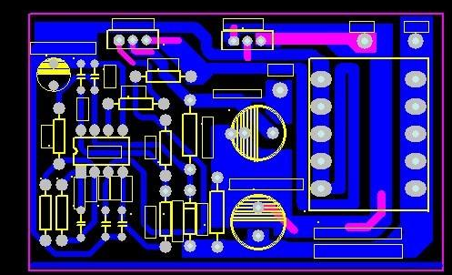
Drawing a four-layer circuit board is one of the most important links in the design process. It includes the pre-planning of the circuit board, the layout and wiring of components and the design verification (DRC) after the circuit board design is completed, and the subsequent gerber and bom tables Waiting for file output and other content, drawing four-layer circuit board design is the most extensive, technical, and difficult link in circuit board design. Therefore, beginners encounter the most problems in PCB design.One, how to add a pad to the networkQuestion: How to add a pad to the network? Answer: To add a pad to a network on the circuit board, there are two specific methods of operation. The first method is to add the pad to the circuit board and then double-click the pad to pop up the Pad dialog box. Use the mouse to click the Advanced icon to enter the Advanced tab, and then select the pad in the drop-down list behind the Net option The network label, and finally click 0K in the dialog box to confirm, you can add the pad to the network. Next, move the modified pad to the network as it is. The second method is to execute the menu command to place the pad, and then directly place the pad on the net where the pad needs to be placed. At this time, the system will automatically add the net label to the pad. After placing a pad, the system is still in the command state of placing pads, and the user can continue to place pads. It is very convenient to use this method to place multiple pads.

Second, about copper pour question 1: What is the role of copper pour? What should be paid attention to in the process of copper pour? Answer: The main function of copper pour is to improve the anti-interference ability of the circuit board and increase the load capacity of the excessive current of the wire. Among them, copper pour the ground wire network is the most common operation. On the one hand, it can increase the conductive area of the ground wire and reduce the common impedance introduced by the circuit due to grounding. On the other hand, it can increase the area of the ground wire and improve the anti-interference of the circuit board. Performance and overcurrent capability. Copper coating should generally follow the following principles. If the component layout and wiring permit, the safety distance between the copper-clad network and other drawings should be more than twice the conventional safety distance; if the component layout and wiring are tight, the safety distance can also be appropriately reduced, But it’s better not to be smaller than "0.5mm". The connection between the copper-clad copper box and the pad with the same network label should be determined according to the specific situation. For example, in order to increase the current-carrying area of the pad, the user should use direct Connection method; if in order to avoid the large-area copper foil heat dissipation too fast when the components are assembled, it should be connected by radiation.Question 2: Why is the copper-clad (copper-clad) file so large? Is there a good solution? Answer: It is normal for the file to have a large amount of data after the copper-clad. But if it is too large, it may be caused by your unscientific settings. If the dialog box is set for copper pour, if the values of the Grid Size and Track Width options are set too small in the dialog box, the circuit board design file will be very large. This is because the copper foil of the copper pour is actually Covered by countless wires, the greater the number of wires, the greater the amount of information stored in the PCB file. In order to prevent the PCB file after copper coating from being too large, the designer can select Grid Size and Track Width. Set a larger value.Question 3: How to remove the separated small pieces of copper in the copper-clad area? Answer: These separated small pieces of copper are what we often call "dead copper". The solution is to open the Polygon Plane dialog box before performing the copper pour operation and select the Remove Dead Copper item, so that the system will automatically remove the "dead copper" when the copper pours.
3. Skills for drawing wires Question 1: How can I make different parts of the same wire have different widths and look continuous and beautiful? Answer: This operation cannot be done automatically, but it can be achieved in several steps using editing skills. Specific operations such as drawing a continuous smooth wire. 1. First place a thin wire with a wire width of 0.5mm, then press the Tab key, in the pop-up wire properties dialog box, modify the wire width to 2mm, and then draw a wire with a width of 2mm. A pad is placed on the wire, and the outer diameter of the pad is the width of the widest wire, which is 2mm.3, use the mouse to select the added pad. 4. Select the menu command Tools/teardrops... The system pops up the Teardrop Options teardrop option setting dialog box. In the Teardrop Options dialog box, the user can set the scope of the teardrop filling operation, adding/removing teardrops, and teardrop filling. Style (including two styles of round and solitary and wire), etc.5, in the dialog box, select the teardrop operation for the selected object, the teardrop style is an arc style, and finally click the OK button to confirm. Teardrop wire is when the guide wire enters the pad or via, its line width gradually increases to form a teardrop shape. The operation of making teardrop wires is called "tear-filling". The purpose of making teardrops on the wires is to strengthen the connection between the wires and the pads (or vias) to prevent the processing of the pads or vias. Causes stress concentration. If the stress concentration is severe, it will often break the wire at the junction of the wire and the weld (or via). Of course, the purpose of smooth and beautiful transition of two sections of wires with different widths can also be achieved before the tears are filled.6, delete the PCB pad to get a wire with smooth connection and natural transition.