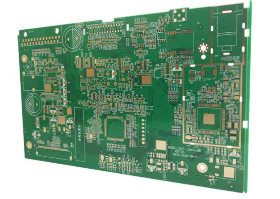
Although there are many theoretical uncertainties in the design of radio frequency (RF) circuit boards, there are still many rules that can be followed in the design of RF circuit boards. However, in the specific design, the real and useful method is when this rule cannot be implemented due to various restrictions, how to develop a compromise solution for them. This article will focus on various problems related to the design of the RF circuit board partition. .
01 Types of micro vias
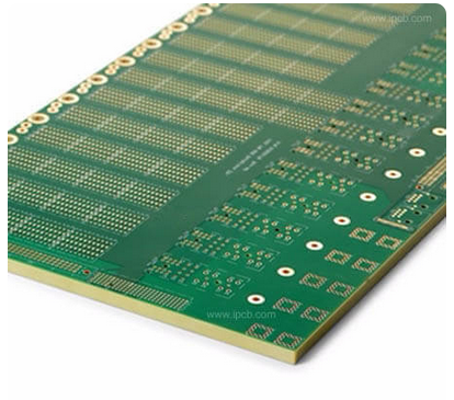
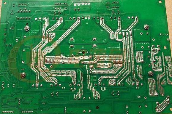
Circuits with different characteristics on high-frequency circuit boardsmust be separated, but if they are not connected under the best conditions that cause interference signals, microvias must be used. Generally, the diameter of micro-vias is 0.05mm~0.22mm. Such vias are generally divided into three categories, namely, blindvia, buryvia and throughvia. Buried holes are located on the upper and lowest surface layers of the printed circuit board. They have a certain depth for the connection between the surface route and the lower inner route. The depth of the hole generally does not exceed a certain ratio (diameter). Buried hole refers to the connection hole located in the inner layer of the printed circuit board, which is not easy to widen to the surface of the PCB circuit board. The two major types of holes are located in the inner layer of the PCB circuit board, and the buried hole forming process is used before lamination. During the whole process of generating the via holes, they will continue to overlap and do a good job of multiple inner layers. The third type is called buried hole. This kind of hole crosses all PCB circuit boards and can be used to complete internal interconnection or as a precision positioning hole for component adhesion.
02 Choose partition method
When designing the RF circuit board, try to protect the high-power RF amplifier (HPA) and low-noise amplifier (LNA). Simply put, let the high-power RF transmitting circuit eliminate the low-noise receiving circuit. If there is a lot of indoor space on the PCB, this can be easily ensured. However, when there are many parts and components, the indoor space of PCB manufacturing will not be large, so it cannot be done. Can put them on both sides of the PCB board, or let them replace the work, rather than another work. Sometimes high-power circuits can also include RF buffers and voltage-controlled oscillators (VCO).
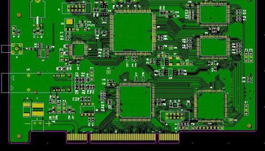
The design partition can be divided into physical partitioning and electrical partitioning. The key to physical partitioning involves the reasonable layout, orientation, and shielding of components; electrical equipment partitions can be divided into power distribution, RF wiring, more sensitive circuits and data signals, and grounding devices.
03 physical partition
A reasonable layout of components is important to complete an excellent RF design. The most effective technique is to fix the components located on the relative path of the RF first and adjust their direction to minimize the length of the relative path of the RF. And make the RF input to eliminate RF output, and try to eliminate high-power circuits and low-noise circuits.
The most effective circuit board stacking method is to distribute the main grounding device on the second layer below the surface, and try to put the RF line on the surface. Minimizing the via size on the RF relative path can not only reduce the relative path inductance, but also reduce the empty solder joints on the main ground plane, and reduce the chance of RF kinetic energy leaking to other areas in the stack.
In the physical indoor space, linear circuits like multi-level amplifiers can generally shield several RF zones from each other, but duplexers, mixers, and high-frequency amplifiers have always had several RF/IF data signals with each other. Impact, so care must be taken to minimize this hazard. RF and IF wiring should be crossed as far as possible, and a total area of grounding device should be separated as far as possible between them. Proper RF relative path is very critical to the characteristics of a whole PCB board, which is why the reasonable layout of components generally accounts for most of the time in the mobile phone PCB board design.
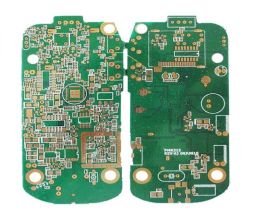
On the mobile phone PCB board, it is generally possible to put the low-noise amplifier circuit on one side of the PCB proofing board, and the high-power amplifier on the other side, and finally means that the duplexer connects them to the RF wireless antenna on the same surface. One end of the CPU and the other end of the baseband CPU. This requires some methods to ensure that the RF kinetic energy does not easily mean vias, which are transmitted from one side of the board to the other. The common technique is to apply buried vias on both sides. It can mean that the buried vias are allocated to areas where the double-sided PCB is not affected by RF, so as to minimize the harmful effects of vias.

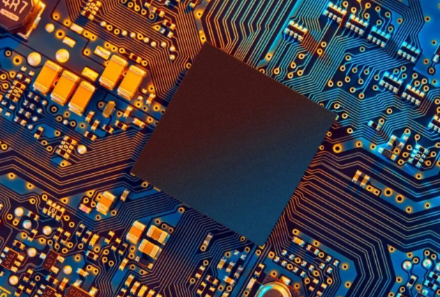
04 Metal shield
Sometimes, it is unlikely to keep sufficient differences among several circuit block chains. In such situations, it is necessary to consider the use of a metal shield to shield the frequency radiation kinetic energy in the RF area, but the metal shield is also defective. Responses, such as: manufacturing costs and installation costs are high.
The metal shielding cover with irregular appearance design cannot ensure high precision during production. The square or square metal shielding cover also restricts the reasonable layout of components; the metal shielding cover is not good for the replacement of components and the movement of common faults; because of the metal shielding The cover must be welded to the road surface, and must maintain a proper distance from the components, so it must occupy the precious indoor space of the PCB board.
It is very important to ensure the details of the metal shield as much as possible. Therefore, the large digital power line entering the metal shield should be routed as far as possible in the inner layer, and it is best to set the next layer of the data signal route layer to a grounded structure. The RF power line can be routed from the small gap at the bottom of the metal shield and the wiring layer at the opening of the grounding device, but the periphery of the opening should be surrounded by the total area of many grounding devices as much as possible. The grounding device on the different data signal layer can be routed. It means that several vias are connected together. Despite the above drawbacks, the metal shield is still very reasonable and is often the only solution to protect important circuits.
05 Power decoupling circuit
Appropriate and reasonable integrated ic power decoupling (decouple) circuit is also critical. Many RF integrated ICs that incorporate linear routes are very sensitive to the noise of the power supply. Generally, each integrated IC must select up to four capacitors and a protective inductor to filter out all power supply noise.
The minimum capacitor value generally lies in the capacitor's own series resonance and pin inductance, and the value of C4 is chosen accordingly. The values of C3 and C2 are relatively large due to the correlation of their own pin inductances, and the actual effect of RF decoupling is worse, but they are more suitable for filtering out lower frequency noise data signals. The RF decoupling is performed by the inductor L1, which prevents the RF data signal from being coupled to the integrated IC from the power plug. Since all the wiring is a potential wireless antenna that can accept and send RF data signals, it is necessary to protect the RF signals from key circuits and components.
The physical location of such decoupling components is generally also important. The reasonable layout standards for these many key components are: C4 must be as close to the IC pin and grounding device as possible, C3 must be close to C4, C2 must be close to C3, and the connection wiring between the IC pin and C4 should be as short as possible. The grounding device end (especially C4) should generally mean that the first grounding structure under the surface is connected to the grounding device foot of the integrated ic. The via hole connecting the component and the ground structure should be as close as possible to the component solder layer on the PCB board. It is best to use the buried hole on the solder layer to minimize the inductance of the electrode connection line. The inductance L1 should be close to C1.
An integrated circuit board or amplifier often has a collector junction output (opencollector), so a pullup inductor (pullupinductor) is necessary to show a high characteristic impedance RF load and a low characteristic impedance DC stabilized power supply, the same standard is also It is applicable to decoupling the power end of this inductor. Some integrated ICs must have several power supplies before they can work, so two or three sets of capacitors and inductors will be required to decouple them. If there is not enough indoor space around the integrated IC, the actual effect of decoupling will be Bad. In particular, it must be noted that there are very few inductances that are parallel to each other. Since this will produce an air-core transformer and cause electromagnetic interference by mutual magnetic induction, the distance between them must be at least equal to the height and width of one of them. Ratio, or order at an oblique angle to minimize its mutual inductance.