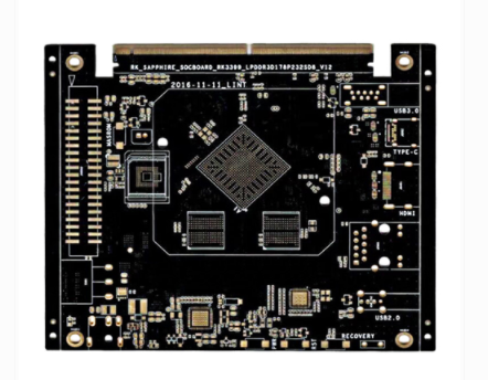
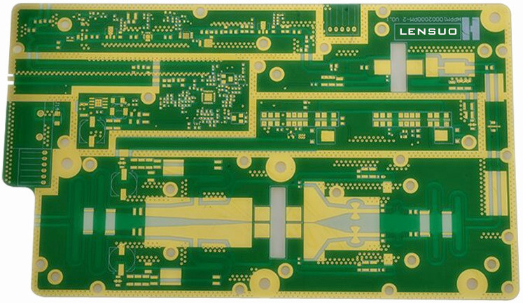
High-frequency mixed-voltage circuit board, high-precision high-frequency circuit board manufacturer
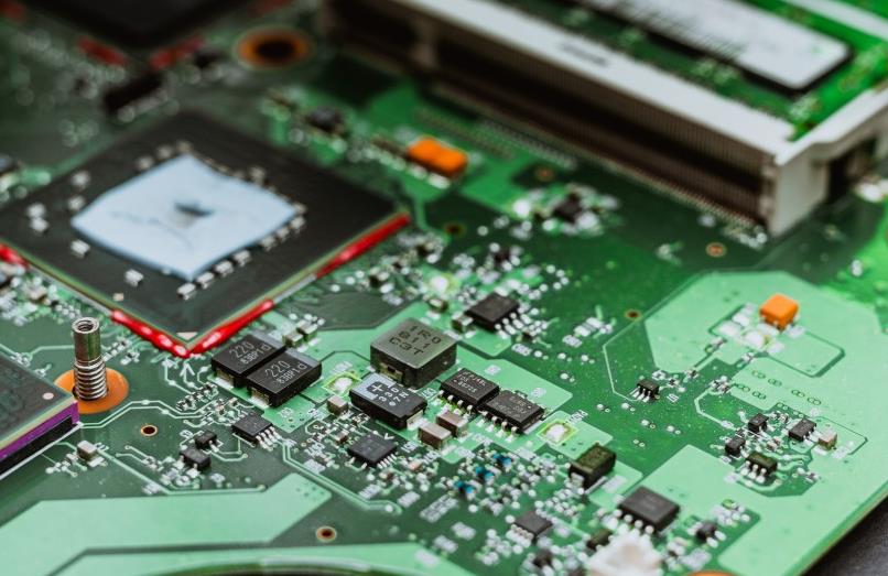
High-precision high-frequency circuit boardmanufacturers in high-speed PCB design, via hole preset is a key factor, it is composed of the hole, the pad area around the hole and the POWER layer isolation area, generally divided into blind holes, buried holes and through holes. Three types of holes. After analyzing the parasitic capacitance and parasitic inductance of the vias during the PCB preset process, the items that should be paid attention to in the high-speed PCB via presets are summarized. Although the size of the pads and vias has gradually decreased, if the thickness of the board is not proportionally reduced, the aspect ratio of the through hole will increase, and the increase of the aspect ratio of the through hole will reduce the reliability. With the maturity of advanced laser drilling technology and plasma dry etching technology, it becomes possible to apply non-through small blind holes and small buried holes. If the diameter of these non-through vias is 0.3mm, the resulting The parasitic parameter variable is about 1/10 of the initial common sense hole, which increases the reliability of the PCB. The vias in the PCB are made of multi-layer circuit boards with blind and buried vias.
Because of the continuous innovation of PCB products, we are ushering in the spring of printed circuit development one after another. The edge of smart phones brings the climax of embedded component printed boards, LED energy-saving lighting will bring the climax of metal-based printed boards, and e-books and film revealers will bring the climax of flexible circuit boards. High-precision high-frequency circuit boards
The innovation of printed circuit is based on technological reform. The traditional technology of PCB production is the copper foil etching method (subtraction method), that is, the copper-clad insulating substrate is etched by a chemical solution to remove the unnecessary copper layer, leaving the required copper conductor type into the circuit pattern; for double-sided and The interlayer interconnection of the multilayer board is successfully connected by drilling and copper electroplating. Nowadays, this traditional process is difficult to be suitable for the manufacture of micron-level thin-circuit HDI boards, it is difficult to successfully achieve rapid and low-cost production, and it is difficult to achieve the goals of energy saving, emission reduction, and green production. The only way to implement technological reform is to change the state.

The circuit connection of the multi-layer board is through buried via and blind via technology. Most motherboards and exposed cards use 4-layer PCB boards, but it is somewhat appropriate to use 6-layer, 8-layer, or even 10-layer PCB boards. If you want to see that the PCB has several layers, you can identify it by carefully inspecting the via holes. Because the 4-layer board used on the motherboard and the display card is the first and fourth layers of wiring, the other layers have other uses (ground Line and power supply). Therefore, as with the double-layer board, the via hole will penetrate the PCB board. If some vias are exposed on the front side of the PCB but cannot be found on the back side, then it must be a 6/8-layer board. If the same via holes can be found on both sides of the PCB, it is naturally a 4-layer board. High-precision high-frequency circuit board
The production process of the foil-clad board is to impregnate glass fiber cloth, glass fiber mat, paper and other reinforcing materials with epoxy resin, phenolic natural resin and other adhesives, and bake it to stage B at a suitable temperature to obtain a pre-impregnated material (abbreviated as Dipping material), and then laminate them with copper foil according to the process requirements, and heat and increase the pressure on the laminator to obtain the required copper clad laminate. High-precision high-frequency circuit board
1. Classification of copper clad laminates Copper clad laminates are composed of three parts: copper foil, reinforcing materials, and adhesives. Sheets are generally classified according to the reinforcement material category and the adhesive category or the special properties of the sheet.
1. According to the classification of reinforcing materials, the most commonly used reinforcing materials for copper clad laminates are alkali-free (alkali metal oxide content not exceeding 0.5%) glass fiber products (such as glass cloth, glass mat) or paper (such as wood pulp paper, Whitening wood pulp paper, cotton lint paper), etc. Because of this, copper clad laminates can be divided into two categories: glass cloth base and paper base.
2. According to the type of adhesive, the adhesives used in the foil-clad laminates are mainly phenolic, epoxy, polyester, polyimide, polytetrafluoroethylene natural resin, etc., because of this, the foil-clad laminates are also divided into phenolic, ring Oxygen type, polyester type, polyimide type, polytetrafluoroethylene type foil clad board.
3. According to the special nature of the base material and its application, it can be divided into general type and self-extinguishing type according to the degree of combustion of the base material in the flame and after leaving the fire source; it can be divided into rigidity and flexibility according to the degree of buckling of the base material Foil-clad laminate: According to the office temperature and office background conditions of the substrate, it can be divided into heat-resistant, anti-radiation, and high-frequency foil-clad laminates. In addition to this, there are also foil-clad laminates used in special occasions, such as prefabricated inner-layer foil-clad laminates, metal-based foil-clad laminates, and can be divided into copper foil, nickel foil, silver foil, aluminum foil, and constantan foil according to the type of foil material., Beryllium copper foil clad laminate.
Definition of special characteristic impedance: at a certain frequency, the resistance of the high-frequency signal or electromagnetic wave in the process of wide spread in the transmission signal line of the electronic component relative to a certain reference layer is called the special characteristic impedance. It is the whole of a vector of electrical impedance, inductive reactance, capacitive reactance...
Classification of special nature impedance:
Up to now, the common special characteristics of impedance are divided into: single-ended (line) impedance, differential (dynamic) impedance, coplanar impedance and so on.
Single-ended (line) impedance: English single ended impedance refers to the measured impedance of a single signal line.
Differential (dynamic) impedance: English differential impedance refers to the impedance measured in two transmission lines of equal width and equal spacing during differential drive.
Coplanar impedance: English coplanar impedance refers to the impedance measured when the signal line is transmitted between GND/VCC (the signal line is equal to the GND/VCC on both sides).
Impedance control required voting conditions: When the signal is transmitted in the PCB wire, if the length of the wire is close to 1/7 of the signal wavelength, the wire at this time becomes a signal transmission line, and the ordinary signal transmission line needs to be impedance Choke down. When PCB is manufactured, it is required to vote whether the impedance needs to be managed and controlled according to the customer's request. If the customer requires impedance control for a certain front line width, the impedance of the line width needs to be managed and controlled during production. High-precision high-frequency circuit board
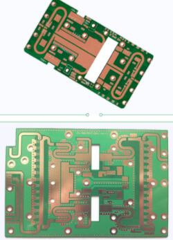
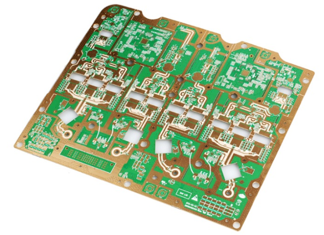
The final results of the trial production show that the prefabrication of multilayer high-frequency mixed-pressure circuit boards is based on one or more factors of cost saving, increased buckling strength, and electromagnetic interference suppression. It must be considered appropriate and the natural resin flow during the pressing process must be used. Low-performance high-frequency prepregs and FR-4 substrates with smoother media appearance. Under such circumstances, there is a greater risk of controlling the adhesion of the product during the pressing process. High-frequency circuit board experiments show that the use of key technologies such as selection of FR-4 A material, pre-set of spherical flow glue baffle block on the edge of the board, application of pressure relief materials, and the use of key technologies such as pressure parameter control system have successfully realized The adhesion between the mixed materials is satisfactory, and the reliability of the circuit board is not abnormal after testing. The material of high-frequency circuit boards for electronic communication products is indeed a good choice.