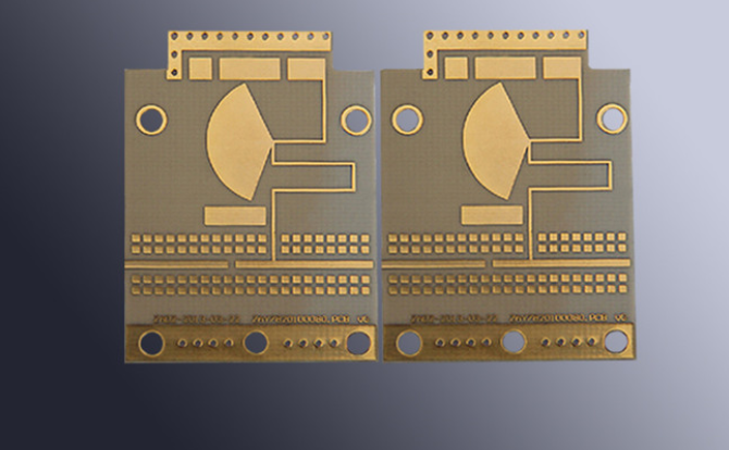
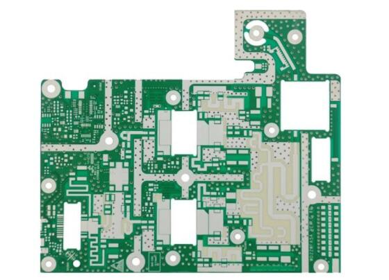
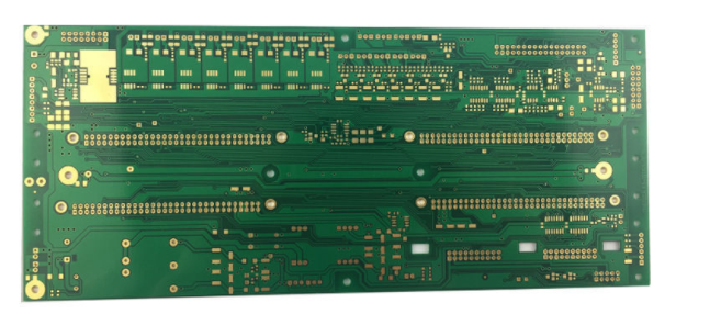
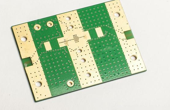
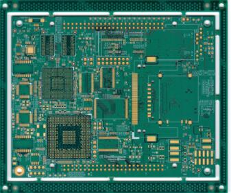
11 tips on high-frequency circuit board wiring
1. High-frequency lines are very concerned about impedance matching and routing. But if you can, you can make exactly the same according to the manufacturer's reference design. After all, the manufacturer's design has undergone a more comprehensive calculation.
2. When you first draw the PCB, please do not arrange your high-frequency traces according to the ordinary signal lines. It is the right way to obtain the reference design from the chip manufacturer. The general chip data manual or related manuals will have high-frequency parts. The wiring reference.
3. The entire high-frequency part can be dotted with more vias to increase ground connectivity. The ground copper has a great influence on the high-frequency wiring. If it is not properly routed, the power supply or other signal lines will have 100k-300K interference signals.
4. Remember not to separate the ground, at least make sure that one side of the ground is a complete ground. Ensure that one side of the ground can be fully copper-clad, and do not separate it with signal lines.

5. Do not place a crystal oscillator next to high-frequency traces. High frequency affects high frequency, this is common sense, try to keep it as far away as possible. Of course, other signal lines should not be too close to the high-frequency line, as the high frequency also affects the low frequency.
6. Place vias next to high-frequency traces to effectively improve signal quality. The high frequency itself should need a shielding cover or shielding layer, but the shielding cover cannot be provided when the circuit board is routed. At this time, the PCB itself can only be used to make a shielding layer. The via can be understood as that shielding layer. The ground below is another layer. The above may not be able to increase the shielding, because it needs to be exposed for debugging.
7. Whether it is the drawing of the schematic diagram or the design of the PCB copy board, it should be considered from the high-frequency working environment in which it is located, in order to be able to design a more ideal PCB copy board.
8. Almost every software has automatic layout, but as a PCB engineer, you should abandon him and make layout by yourself to make PCB productionmore effectively and reasonably.
9. Generally, the fixed position components related to the mechanical size are placed first, then special and larger components, and finally small components. At the same time, it is necessary to take into account the requirements of wiring, the placement of high-frequency components should be as compact as possible, and the wiring of signal lines can be as short as possible, thereby reducing cross-interference of signal lines.
10. The original is generally not too close to the edge, preferably 3-5mm. Power sockets, switches, interfaces between PCB copy boards, indicator lights, etc. are all positioning plug-ins related to mechanical dimensions. Generally, the interface between the power supply and the PCB is placed on the edge of the PCB, and there should be a distance of 3mm to 5mm from the edge of the PCB; the light-emitting diodes should be placed accurately according to the needs; switches and some fine-tuning components, such as adjustable inductance, Adjusting resistors, etc. should be placed near the edge of the PCB for easy adjustment and connection; components that need to be replaced frequently must be placed in a location with fewer components for easy replacement.
11. Whether the layout is reasonable or not directly affects the product's life, stability, EMC (electromagnetic compatibility), etc. It must be based on the overall layout of the circuit board, the operability of the wiring and the manufacturability of the PCB copy board, mechanical structure, and heat dissipation., EMI (electromagnetic interference), reliability, signal integrity and other aspects are comprehensively considered.