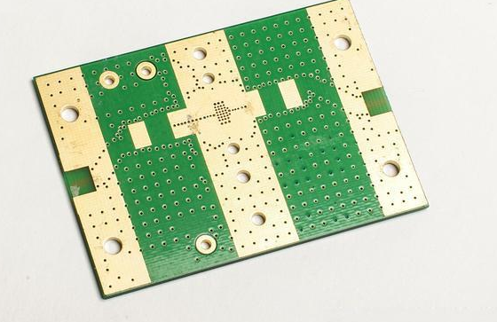
High-Frequency Ceramic Substrate (also known as a ceramic circuit board) has the characteristics of high thermal conductivity, good heat resistance, low thermal expansion coefficient, high mechanical strength, good insulation, corrosion resistance, radiation resistance, and so on, and has been widely used in the packaging of electronic devices.
The first generation of semiconductors, represented by silicon (Si) and germanium (Ge) materials, were mainly applied in the field of data operation, which laid the foundation of the microelectronics industry. The second-generation semiconductors, represented by GaAs and InP, are mainly used in the communication field and are used to make high-performance microwave, millimeter, and light-emitting devices, laying the foundation of the information industry. With the development of technology and the continuous extension of application needs, the limitations of the two are gradually reflected, and it is difficult to meet the requirements of high frequency, high temperature, high power, high energy efficiency, harsh environment resistance, and lightweight miniaturization.

The third-generation semiconductor materials represented by silicon carbide (SiC) and gallium nitride (GaN) have the characteristics of the large bandgap, high critical breakdown voltage, high thermal conductivity, high carrier saturation drift speed, and so on. The electronic devices made by them can work stabilities at 300°C or even higher temperatures (also known as power semiconductors or high-temperature semiconductors). It is the "core" of the solid-state light source (such as LED), laser (LD), power electronics (such as IGBT), focused photovoltaic (CPV), microwave radio frequency (RF), and other devices. It has broad application prospects in semiconductor lighting, automotive electronics, the new generation of mobile communications (5G), new energy and new energy vehicles, high-speed rail transit, consumer electronics, and other fields. It is expected to break through the bottleneck of traditional semiconductor technology and complement the first and second-generation semiconductor technology. It has important application value in optoelectronic devices, power electronics, automotive electronics, aerospace, deep good drilling, and other fields, and will play an important role in energy conservation and emission reduction, industrial transformation and upgrading, and the birth of new economic growth points.
With the continuous development of power devices (including LED, LD, IGBT, CPV, etc.), heat dissipation has become a key technology affecting device performance and reliability. For electronic devices, the typical 10°C temperature increase reduces the device life by 30% to 50%. Therefore, the selection of appropriate packaging materials and technology and the improvement of heat dissipation capability of the device become the technical bottleneck of the development of power devices. Taking high-power LED packaging as an example, 70% ~ 80% of the input power is converted to heat (only about 20% ~ 30% is converted to light energy), the LED chip area is small, and the device power density is large (more than 100 W/cm2). Therefore, heat dissipation becomes a key problem to be solved in high-power LED packaging. If not timely chip fever export and dissipation, a lot of heat will gather in the LED inside, chip junction temperature will gradually rise, on the one hand, the LED performance (such as lower luminous efficiency, wavelength redshift, etc.), on the other hand, it will produce thermal stress inside the LED device, cause a series of reliability problems (such as service life, temperature change, etc.).
The packaging substrate mainly uses the high thermal conductivity of the material itself to export the heat from the chip (heat source) and realize the heat exchange with the external environment. For power semiconductor devices, the packaging substrate must meet the following requirements:
(1) High thermal conductivity. At present, power semiconductor devices are packaged with thermoelectric separation. Most of the heat generated by devices is transmitted through the packaging substrate. The substrate with good thermal conductivity can prevent the chip from thermal damage.
(2) Matching with the thermal expansion coefficient of chip material. The power device chip itself can withstand high temperatures, and the current, environment, and working conditions will change its temperature. Since the chip is directly mounted on the packaging substrate, the matching of the thermal expansion coefficient can reduce the thermal stressz of the chip and improve the reliability of the device.
(3) Good heat resistance, meet the high-temperature use requirements of power devices, with good thermal stability.
(4) Good insulation, to meet the requirements of electrical interconnection and insulation of devices.
(5) High mechanical strength, meet the strength requirements of device processing, packaging, and application process.
(6) The price is suitable for mass production and application.
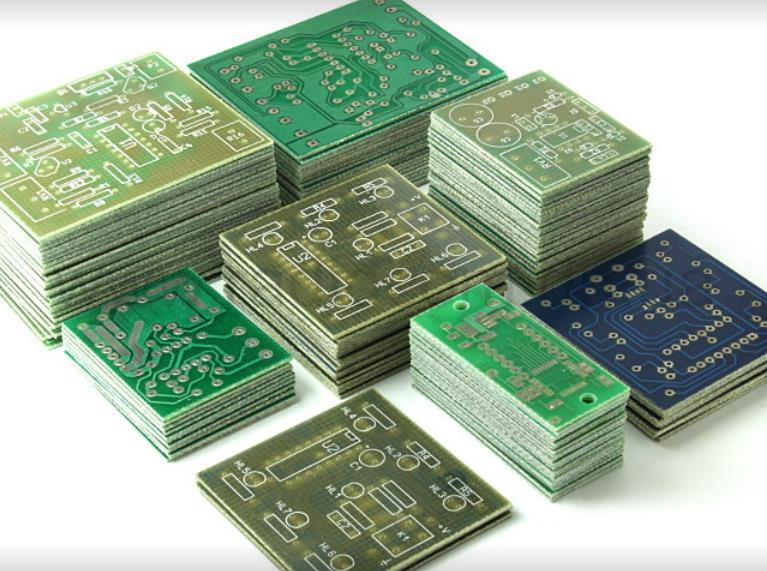
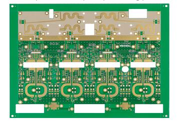
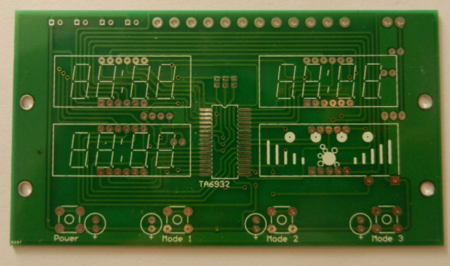
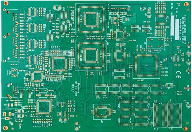
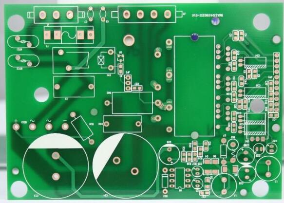
At present, the commonly used electronic packaging substrates can be divided into polymer substrates, metal substrates (metal core circuit board, MCPCB), and ceramic substrates. For power device packaging, the packaging substrate not only has the basic wiring (electrical interconnection) function but also requires high thermal conductivity, heat resistance, insulation, strength, and heat matching performance. Therefore, the use of polymer substrate (such as PCB) and metal substrate (such as MCPCB) is very limited; The ceramic material itself has high thermal conductivity, good heat resistance, high insulation, high strength, and chip material thermal matching performance, is very suitable for power device high-frequency ceramic substrate, has been widely used in semiconductor lighting, laser and optical communication, aerospace, automotive electronics, deep-sea drilling and other fields.