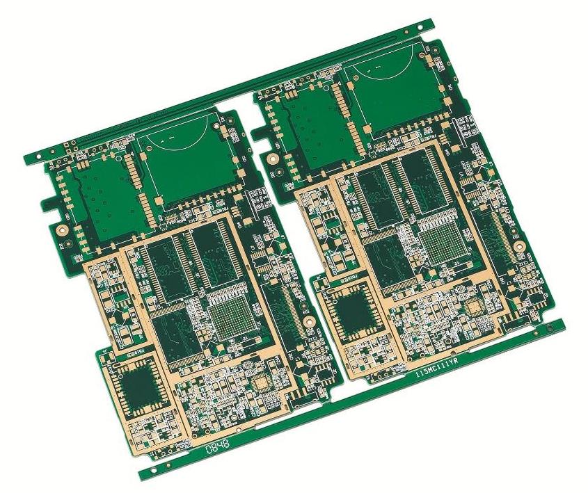
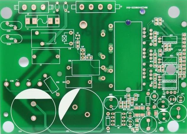
In reverse technology research PCB circuit board, a reverse schematic diagram refers to a circuit diagram drawn by the file diagram or directly according to the product object, aiming to explain the principle and work of the circuit board. Moreover, the circuit diagram is also used to analyze the functional characteristics of the product itself. In forward design, the general product development should first carry out schematic design, and then according to the schematic design PCB design.Whether it is used to analyze circuit board principle and product working characteristics in reverse research or used as the basis of PCB design in forwarding design, PCB schematic has a special role. So, according to the document or object, how to carry out the PCB schematic diagram back, the back process should pay attention to those details?
1., Reasonable division of functional areas
When reverse designing the schematic diagram of an intact PCB, reasonable division of functional areas can help engineers reduce some unnecessary trouble and improve the efficiency of drawing. Generally speaking, components with the same function on a PCB circuit board will be arranged centrally, so that the functional division of areas can provide a convenient and accurate basis for reverting the schematic diagram.
However, the division of this functional area is not arbitrary. It requires engineers to have a certain understanding of electronic circuit-related knowledge. First of all, find out the core components of a functional unit, and then according to the wiring connection can be traced to find out the other components of the same functional unit, the formation of a functional partition. The formation of functional partition is the basis of the schematic drawing. In addition, don't forget to use the component number on the circuit board to help you partition functions faster.

2, Correctly distinguish lines, reasonable drawing wiring
For the distinction of ground wire, power line, and signal line, engineers also need to have relevant knowledge of power supply, circuit connection, PCB wiring, and so on. The distinction of these circuits can be analyzed from the connection of components, the width of copper foil, and the characteristics of electronic products themselves.
In the wiring drawing, to avoid line crossing and interspersing, the ground can use a large number of grounding symbols, all kinds of lines can use different colors of different lines to ensure clear discernable, for all kinds of components can also use special signs, and can even separate the unit circuit drawing, and then combined.
3, Find the right reference parts
This reference piece can also be said to be the main part used at the beginning of the schematic drawing. After determining the reference piece, drawing according to the pins of these reference pieces can ensure the accuracy of schematic drawing to a greater extent.
Benchmark for engineers, a sure is not very complicated things, in general, can choose to play a leading role in the circuit components as a benchmark, they generally larger, pin more, convenient drawing, such as integrated circuit, transformer, transistor, etc.
4., Master the basic framework and draw lessons from similar schematic diagrams
For some basic electronic circuit frame composition and principle drawing method, engineers need to master, not only to be able to draw some simple, classic basic composition of the unit circuit directly but also to form the overall frame of the electronic circuit.
On the other hand, it should not be ignored that electronic products of the same type have certain similarities in schematic diagrams. Engineers can fully refer to similar circuit diagrams to deduce new product schematic diagrams based on experience accumulation.
5., Check and optimize
After the schematic drawing is completed, the reverse design of the PCB schematic diagram can be concluded only after testing and checking. The nominal values of components sensitive to PCB distribution parameters need to be checked and optimized. According to the PCB board file diagram, the schematic diagram is compared, analyzed, and checked to ensure that the schematic diagram is completely consistent with the file diagram.