Talking about the 14 common mistakes in PCB boards
1. Common errors in the schematic diagram of the PCB board
(1) There is no signal connected to the ERC report pin:
a. I/O attributes are defined for the pins when the package is created;
b. When creating a component, the pin direction is reversed, and it must be connected to the non-pinname end;
c. Inconsistent grid attributes are modified when components are created or placed, and the pins and wires are not connected;
d. The most common reason is that there is no project file, which is the most common mistake for beginners.
2) The component goes out of the drawing boundary: no component is created in the center of the diagram paper in the component library.
3) When using multi-part components created by yourself, never use annotate.
4) The network table of the created project file can only be partially imported into the PCB: when the netlist is generated, global is not selected.
Two, common errors in PCB boards
(1) It is reported that NODE is not found when the network is loaded
a. The components in the schematic diagram use packages that are not in the PCB library;
b. The components in the schematic diagram use packages with inconsistent names in the PCB library;
c. The components in the schematic diagram use packages with inconsistent pinnumbers in the PCB library.
For example, a triode: the pin numbers in sch are e, b, c, and in PCB boards are 1, 2, 3.
(2) Can not always print on one page when printing
a. It is not at the origin when creating the PCB library;
b. The component has been moved and rotated many times, and there are hidden characters outside the boundary of the PCB board. Choose to show all hidden characters, shrink the PCB, and then move the characters to the boundary.
(3) The DRC reporting network is divided into several parts:
It means that the network is not connected. Look at the report file and use CONNECTEDCOPPER to find it. If you make a more complicated design, try not to use automatic wiring.

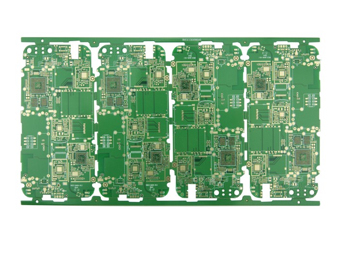
Three, common errors in the PCB manufacturing process
iPCB is a high-tech manufacturing enterprise focusing on the development and production of high-precision PCBs. iPCB is happy to be your business partner. Our business goal is to become the most professional prototyping PCB manufacturer in the world. Mainly focus on microwave high frequency PCB, high frequency mixed pressure, ultra-high multi-layer IC testing, from 1+ to 6+ HDI, Anylayer HDI, IC Substrate, IC test board, rigid flexible PCB, ordinary multi-layer FR4 PCB, etc. Products are widely used in industry 4.0, communications, industrial control, digital, power, computers, automobiles, medical, aerospace, instrumentation, Internet of Things and other fields. For many years, we have been focusing on the production of multi-layer precision circuit boards. We have shared some small experiences in the perfect integration of PCB manufacturing and design.
(1) Pad overlap
a. Causes heavy holes, and breaks the drill and damages the holes due to multiple drilling in one place during drilling;
b. In the multi-layer board, there is both a connection plate and an isolation plate at the same position, and the board has a performance of isolation and connection errors.
(2) Irregular use of graphics layer
a. Violation of conventional design, such as the component surface design in the Bottom layer, and the welding surface design in the TOP layer, causing misunderstanding;
b. There are a lot of design rubbish on each layer, such as broken lines, useless borders, labels, etc.
(3) Unreasonable characters
a. The characters cover the SMD solder tabs, which brings inconvenience to PCB on-off detection and component soldering;
b. The characters are too small, which makes screen printing difficult. If the characters are too large, they will overlap each other and be difficult to distinguish. The font is generally >40mil.
(4) Single-sided pad setting aperture
a. Single-sided pads are generally not drilled, and the aperture should be designed to be zero, otherwise when the drilling data is generated, the coordinates of the hole will appear at this position. Special instructions should be given for drilling;
b. If a single-sided pad needs to be drilled, but the aperture is not designed, the software treats this pad as an SMT pad when outputting electrical and ground data, and the inner layer will lose the isolation disk.
(5) Draw pads with filling blocks
Although it can pass the DRC inspection, the solder mask data cannot be directly generated during processing, and the pad is covered with solder mask and cannot be soldered.
(6) The electrical ground layer is designed with both a heat sink and a signal line, and the positive and negative images are designed together, and errors occur.
(7) Large area grid spacing is too small
The grid line spacing is less than 0.3mm. During the PCB manufacturing process, the pattern transfer process will cause film breakage after development, which will increase the processing difficulty.
(8) The graphics are too close to the frame
At least 0.2mm or more spacing should be ensured (V-cut 0.35mm or more), otherwise the copper foil will be warped and the solder resist will fall off during the exterior processing, which will affect the appearance quality (including the inner copper skin of the multilayer board).
(9) The outline frame design is not clear
Many layers are designed with frames and do not overlap, which makes it difficult for PCB manufacturers to determine which line to use. The standard frame should be designed on the mechanical layer or the BOARD layer, and the internal hollowed-out parts should be clear.
(10) Uneven graphic design
When the pattern is electroplated, the current distribution is uneven, which affects the uniformity of the coating, and even causes warpage.
(11) Short shaped hole
The length/width of the special-shaped hole should be> 2:1, and the width should be> 1.0 mm, otherwise the CNC drilling machine cannot process it.
(12) Milling profile positioning hole is not designed
If possible, design at least two positioning holes with a diameter of> 1.5mm in the PCB board.
(13) The aperture is not clearly marked
a. Combine the apertures that may be combined into a reservoir area as much as possible;
b. The aperture marking should be marked in metric system as much as possible, and in increments of 0.05;
c. Whether the tolerances of metallized holes and special holes (such as crimp holes) are clearly marked.
(14) Unreasonable wiring in the inner layer of the multilayer circuit board
a. There are gaps in the design of the isolation belt, which is easy to misunderstand;
b. The isolation band design is too narrow to accurately judge the network;
c. The heat dissipation pad is placed on the isolation tape, and it is easy to fail to connect after drilling.