What method can be adopted in the process of PCB processing design to effectively avoid electromagnetic interference? Let's take a look with the editor.
Anti-interference is a very important part of modern PCB design, which directly reflects the performance and reliability of the entire system. For PCB design engineers, anti-interference design is the key and difficult point that everyone must master.
1, the existence of interference in the PCB board
In actual research, it is found that there are four main interferences in PCB board design: power supply noise, transmission line interference, coupling and electromagnetic interference (EMI).
1. Power supply noise
In high-frequency circuits, power supply noise has a significant impact on high-frequency signals. Therefore, first of all, the power supply requires low noise. Here, a clean ground is as important as a clean power source.
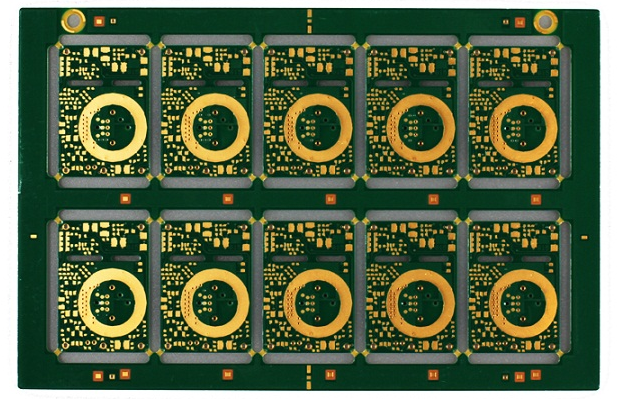
PCB processing design
2. Transmission line
There are only two types of transmission lines in PCB: strip line, microwave line and transmission line. The big problem is reflection, which can cause many problems. For example, the load signal will be the superposition of the original signal and the echo signal, which will increase the difficulty of signal analysis; the reflection will cause return loss, and the effect on the signal will be as serious as the additive noise interference.

3. Coupling
The interference signal generated by the interference source causes electromagnetic interference to the electronic control system through a certain coupling channel.
The coupling method of interference is nothing more than acting on the electronic control system through wires, spaces, public lines, etc. The analysis mainly includes the following types: direct coupling, common impedance coupling, capacitive coupling, electromagnetic induction coupling, radiation coupling, etc.
4. Electromagnetic interference
Electromagnetic interference EMI includes conducted interference and radiated interference. Conducted interference refers to the coupling (interference) of a signal from one power grid to another power grid through a conductive medium.
Radiated interference refers to the interference source coupling (interference) its signal to another power grid through space.
In the design of high-speed PCBs and systems, high-frequency signal lines, integrated circuit pins and various connectors may become sources of radiation interference with antenna characteristics, which will emit electromagnetic waves and affect other systems or other subsystems in the system. normal work.
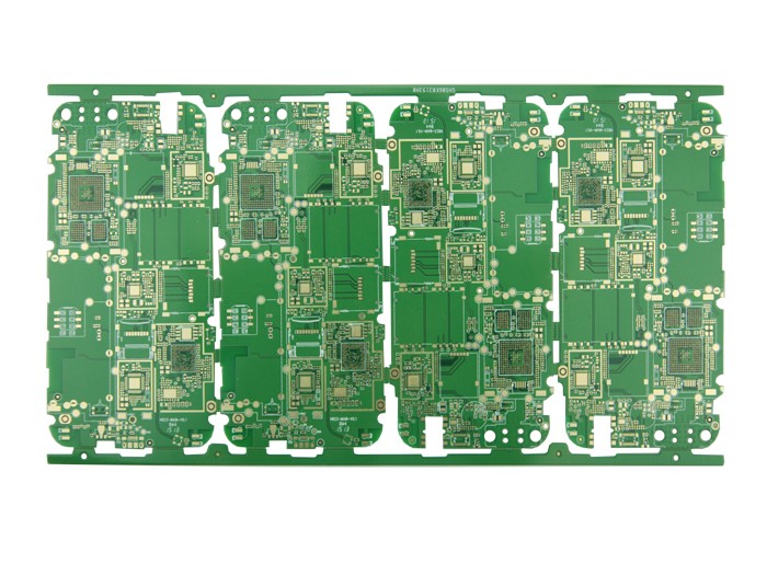
PCB processing plant
2. PCB design anti-interference measures
The anti-interference design of the printed circuit board is closely related to the specific circuit. Next, we only explain some common PCB anti-interference design measures.
1. Power line design
According to the current of the printed circuit board, try to rent the width of the power cord to reduce the loop resistance. At the same time, the direction of the power line and the ground line is consistent with the direction of data transmission, which helps to enhance the anti-noise ability.
2. PCB design ground wire design principle
(1) The digital ground is separated from the analog ground. If there are both logic circuits and linear circuits on the circuit board, they should be separated as much as possible. The grounding of the low-frequency circuit should be grounded in parallel at a single point as much as possible. When there are difficulties in actual wiring, you can connect them in series and then connect them in parallel. The high-frequency circuit should be grounded in series with multiple points, the grounding wire should be short and leased, and the grid-like large-area grounding foil should be used as far as possible around the high-frequency components.
(2) The ground wire should be as thick as possible. If the ground wire is made of a very thin wire, the ground potential will change as the current changes, thereby reducing noise immunity. Therefore, the ground wire should be thickened so that it can pass three times the allowable current on the printed circuit board. If possible, the ground wire should be 2 ~ 3 mm or more.
(3) The grounding wire forms a closed loop. For a printed board composed of only digital circuits, arranging the grounding circuits of the digital circuits into groups of loops can improve the anti-noise ability.
3. Configuration of decoupling capacitors
One of the common practices in PCB design is to configure appropriate decoupling capacitors in all key parts of the PCB. The general configuration principles of decoupling capacitors are:
(1) Connect a 10 ~ 100uf electrolytic capacitor across the power input terminal. If possible, it is better to connect more than 100uF.
(2) In principle, each integrated circuit chip should be equipped with a 0.01pF ceramic chip capacitor. When the printed board gap is insufficient, every 4 to 8 chips can be equipped with a 1-10pF tantalum capacitor.
(3) For devices with weak anti-noise ability and large power changes during shutdown, such as RAM and ROM storage devices, the decoupling capacitor should be directly connected between the power line and the ground line of the chip.
(4) Capacitor leads should not be too long, especially high-frequency bypass capacitors should not have leads.
4. Methods to eliminate electromagnetic interference in PCB design
(1) Reduce loops: Each loop is equivalent to an antenna, so we need to minimize the number of loops, the area of the loop, and the antenna effect of the loop. There is only one loop to ensure the signal...at any two points, avoid artificial loops, and use as many power planes as possible.
(2) Filtering: There are three ways to filter power lines and signal lines to reduce EMI: decoupling capacitors, EMI filters and magnetic components.
(3) Shielding.
(4) Reduce the speed of high-frequency devices as much as possible.
(5) Increasing the dielectric constant of the PCB board can prevent the high-frequency parts such as the transmission line near the board from radiating outward; increasing the thickness of the PCB board and reducing the thickness of the microstrip line as much as possible can prevent the electromagnetic line from overflowing and radiating.
The above is the way to eliminate electromagnetic interference in Chengdu PCB processing design to share with you. What else do you want to know? Just leave a message and let us know.