Circuit board proofing production process introduction
The creator of the printed circuit board is the Austrian Paul Eisler (Paul Eisler), in 1936, he first used the printed circuit board in the radio. In 1943, Americans mostly used this technology for military radios. In 1948, the United States officially approved this invention for commercial use. Since the mid-1950s, printed circuit boards have only begun to be widely used.
Before the advent of PCB boards, the interconnection between electronic components was done directly by wires. Nowadays, wires exist only in the laboratory for test applications; printed circuit board proofing has definitely occupied an absolute control position in the electronics industry.
PCB production process:
1. Contact the manufacturer
First, you need to find the circuit board manufacturer on the Internet, and then to understand the company size, product advantages, and address of the circuit board factory, and then communicate (QQ or call). There will be relevant personnel to quote you, place an order, and follow up. Production schedule, shipment, delivery.

2. Cutting
Purpose: According to the requirements of the engineering data MI, on the large sheets that meet the requirements, cut into small pieces to produce panels. Small sheets that meet customer requirements.
Process: large sheet - cutting board according to MI requirements - curium board- beer fillet\grinding - board out
Three, drilling
Purpose: According to the engineering data, drill the required aperture at the corresponding position on the sheet material that meets the required size.
Process: stacked board pin - upper board - drilling - lower board - inspection\repair
Fourth, sink copper
Purpose: Immersion copper is to deposit a thin layer of copper on the insulating hole wall by chemical method.
Process: rough grinding - hanging board - automatic copper sinking line - lower board - dip% dilute H2SO4 - thickened copper
Five, graphics transfer
Purpose: Graphic transfer is to transfer the image on the production film to the board
Process: (blue oil process): grinding plate - printing the first side - drying - printing the second side - drying - exploding - developing shadow - inspection; (dry film process): hemp board - pressing film - standing - right Position-Exposure-Standing-Development-Check
Six, graphic plating
Purpose: Pattern electroplating is to electroplate a copper layer with the required thickness and a gold-nickel or tin layer with the required thickness on the bare copper skin or hole wall of the circuit pattern.
Process: upper board - degreasing - second washing with water - micro-etching - washing - pickling - copper plating - washing - pickling - tin plating - washing - lower board
Seven, remove the film
Purpose: Use NaOH solution to remove the anti-plating coating film to expose the non-circuit copper layer.
Process: water film: insert rack - soak alkali - rinse - scrub - pass machine; dry film: release board - pass machine
Eight, etching
Purpose: Etching is to use a chemical reaction method to corrode the copper layer of non-circuit parts.
Nine, green oil
Purpose: Green oil is to transfer the graphic of the green oil film to the board to protect the circuit and prevent the tin on the circuit when welding parts.
Process: grinding plate-printing photosensitive green oil-curium plate-exposure-exposure; grinding plate-printing the first side-drying plate-printing the second side-drying plate
Ten, characters
Purpose: Characters are provided as a mark for easy identification
Process: After the green oil finishes - cool and stand - adjust the screen - print characters - rear curium
Eleven, gold-plated fingers
Purpose: to plate a layer of nickel/gold with the required thickness on the finger of the plug to make it more hard and wear-resistant
Process: upper plate - degreasing - washing twice - micro-etching - washing twice - pickling - copper plating - washing - nickel plating - washing - gold plating
Tin plate (a process in parallel)
Purpose: Tin spraying is to spray a layer of lead tin on the exposed copper surface that is not covered with solder mask to protect the copper surface from corrosion and oxidation to ensure good soldering performance.
Process: micro-erosion - air drying - preheating - rosin coating - solder coating - hot air leveling - air cooling - washing and air drying
12. Forming
Purpose: through die stamping or CNC gong machine gong forming the shape required by the customer. Organic gong, beer board, hand gong, hand cutting
Note: The accuracy of the data gong machine board and the beer board is higher. The hand gong is second, and the minimum hand-cutting board can only make some simple shapes.
13. Test
Purpose: To pass electronic 100% testing to detect defects that affect functionality such as open circuits and short circuits that are not easy to find visually.
Process: upper mold - release board - test - pass - FQC visual inspection - unqualified - repair - return test - OK - REJ - scrap
14. Final inspection
Purpose: To pass 100% visual inspection of board appearance defects, and to repair minor defects to avoid problems and defective boards from flowing out.
Specific work flow: incoming materials - view information - visual inspection - qualified - FQA spot check - qualified - packaging - unqualified - processing - inspection OK
15. Vacuum packaging
16. Shipment
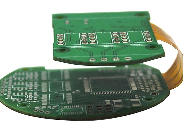
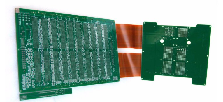
iPCB is a high-tech manufacturing enterprise focusing on the development and production of high-precision PCBs. iPCB is happy to be your business partner. Our business goal is to become the most professional prototyping PCB manufacturer in the world. Mainly focus on microwave high frequency PCB, high frequency mixed pressure, ultra-high multi-layer IC testing, from 1+ to 6+ HDI, Anylayer HDI, IC Substrate, IC test board, rigid flexible PCB, ordinary multi-layer FR4 PCB, etc. Products are widely used in industry 4.0, communications, industrial control, digital, power, computers, automobiles, medical, aerospace, instrumentation, Internet of Things and other fields.