The development of PCB layout technology
In the early circuit board design tools, there were special layout software for layout and special wiring software for wiring. There was no connection between the two. With the application of high-density single-chips, high-density connectors, microvia built-in technology, and 3D boards in the design of printed circuit boards for ball grid array packaging, layout and wiring have become more and more integrated and have become an important part of the design process. component .
Software technologies such as automatic layout and free-angle wiring have gradually become important methods to solve such highly integrated problems. Using such software, manufacturable circuit boards can be designed within a specified time frame. In the current situation where the time to market for products is getting shorter and shorter, manual wiring is extremely time-consuming and untimely. Therefore, place and route tools are now required to have an automatic routing function to quickly respond to the market's requirements for product design.

3D tools are used for layout and routing of irregular and shaped boards that are increasingly widely used. For example, Zuken's Freedom latest tool uses a three-dimensional base plate model to carry out the spatial layout of the components, followed by two-dimensional wiring. This process can also tell: Is the board manufacturable?
In the future, design methods such as using shaded differential pairs on two different layers will become increasingly important, routing tools must also be able to handle this design, and signal rates will continue to increase.
There are also tools that integrate placement and routing tools with advanced simulation tools for virtual prototypes, such as Zuken’s Hot Stage tool, so routing issues can be considered even during virtual prototypes.
Now, automatic wiring technology has become extremely popular. We believe that new software technologies such as free-angle routing, automatic layout, and 3D layout will also become the daily design tools of board designers like automatic routing technology. Designers can use these new tools to solve new types of microvias and monolithic high-density integrated systems. Hardware technical issues.
Free angle wiring
As more and more functions are integrated on a monolithic device, the number of output pins has also greatly increased, but the package size has not been expanded accordingly. Therefore, coupled with the limitations of pin spacing and impedance factors, such devices must use finer line widths. At the same time, the overall reduction in product size also means that the space for layout and wiring has also been greatly reduced. In some consumer products, the size of the backplane is almost the same as the size of the device on it, and components occupy up to 80% of the board area.
The pins of some high-density components are staggered, and automatic routing cannot be performed even with a tool with a 45° routing function. Although the 45° wiring tool can perform perfect processing on certain line segments that are exactly 45°, the free-angle wiring tool has greater flexibility and can maximize the wiring density.
The pull-tight function enables each node to be automatically shortened after wiring to meet the space requirements. It can greatly reduce signal delay, while reducing the number of parallel paths, helping to avoid crosstalk.
Although the free-angle design is manufacturable and has good performance, this design will cause the motherboard to look less beautiful than the previous design. After the time to market, the motherboard design may no longer be a work of art.
High-density devices
The latest high-density system-on-chips are packaged in BGA or COB, and the pin pitch is decreasing day by day. The ball pitch has been as low as 1mm and will continue to decrease, making it impossible for the package signal lines to be led out using traditional wiring tools. There are currently two ways to solve this problem: one is to lead the signal line from the lower layer through the hole under the ball; the other is to find a lead channel in the ball grid array by using very fine wiring and free-angle wiring. For such high-density devices, it is only feasible to use wiring with extremely small width and space. Only in this way can a higher yield rate be ensured. Modern wiring technology also requires these constraints to be automatically applied.
The free wiring method can reduce the number of wiring layers and reduce product costs. It also means that under the condition of the same cost, some ground planes and power planes can be added to improve signal integrity and EMC performance.
Next-generation circuit board design technology
The application of microporous plasma etching technology in multilayer boards, especially in cellular phones and household appliances, has greatly changed the requirements for layout tools. Using plasma etching to add a new hole in the path width will not increase the bottom plate itself or the manufacturing cost, because for plasma etching, the cost of making a thousand holes is as low as the cost of making a hole (this is the same as the laser The drilling method is very different).
This requires the wiring tool to have greater flexibility. It must be able to apply different constraints and be able to adapt to the requirements of different microvias and construction techniques.
The increasing component density has also had some influence on the layout design. Place and route tools always assume that there is enough space on the board for the component picker and place machine to pick and place surface mount components without affecting the components already on the board. But the sequential placement of components will cause such a problem that every time a new component is placed, the best position of each component on the board will change.
This is why the layout design process is low in automation and high in manual intervention. Although the current layout tools do not have any restrictions on the number of components in sequential layout, some engineers believe that the layout tools are actually limited when they are used in sequential layout. This limit is about 500 components. Some engineers think that when up to 4,000 components are placed on a board, a big problem will arise.
Design constraints
Due to the consideration of electromagnetic compatibility (EMC) and high-density design factors such as electromagnetic interference, crosstalk, signal delay, and differential pair wiring, the constraints on placement and routing are increasing every year. For example, a few years ago, a typical circuit board only needed 6 differential pairs for wiring, but now it needs 600 pairs. It is impossible to realize these 600 pairs of wiring only by manual wiring in a certain period of time, so automatic wiring tools are indispensable.
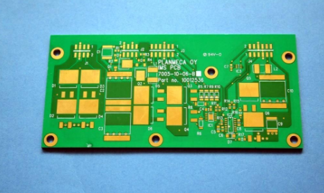
Although compared with a few years ago, the number of nodes (net) in today's design has not changed much, but the complexity of the silicon chip has increased, but the proportion of important nodes in the design has greatly increased. Of course, for some particularly important nodes, place and route tools are required to be able to distinguish them, but there is no need to limit each pin or node. ipcb is a high-precision, high-quality PCB manufacturer, such as: isola 370hr PCB, high-frequency PCB, high-speed PCB, ic substrate, ic test board, impedance PCB, HDI PCB, Rigid-Flex PCB, buried blind PCB, advanced PCB, microwave PCB, telfon PCB and other ipcb are good at PCB manufacturing.