PCB design experience sharing

For electronic products, PCB design is a necessary design process from electrical schematic diagram to a specific product. The rationality of its design is closely related to product production and product quality. For many people who are just engaged in electronic design, they have little experience in this field, although they have learned PCB design software, However, the printed circuit board often has such and such problems, and there are few articles on this in many electronic journals. The author has been engaged in printed circuit board design for many years. Here, I will share some experience of printed circuit board design with you, hoping to play a role in throwing bricks and attracting jade. The author's PCB design software was tango a few years ago, and now protel2.7 for windows is used.
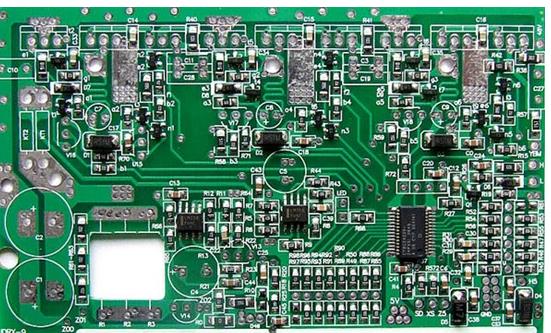
1, Board layout 1. The components on the printed circuit board are usually placed in a fixed position in close coordination with the structure, such as power sockets, indicator lights, switches, connectors, etc. after these components are placed, they are locked with the lock function of the software so that they will not be moved by mistake; Place special components and large components on the line, such as heating elements, transformers, IC, etc.
2. Distance between small components and the edge of the board: if possible, all components and parts shall be placed within 3mm from the edge of the board or at least greater than the thickness of the board. This is because they shall be provided to the guide rail slot during mass production of assembly line plug-ins and wave soldering. At the same time, it is also to prevent edge defects caused by shape processing, If there are too many components on the printed circuit board and it is necessary to exceed the range of 3mm, a 3mm auxiliary edge can be added to the edge of the board, and the V-shaped groove can be opened on the auxiliary edge, which can be broken by hand during production.
Isolation between high and low voltage: there are high voltage circuits and low voltage circuits on many printed circuit boards at the same time. The components of the high voltage circuit shall be separated from the low voltage part, and the isolation distance is related to the withstand voltage. Generally, the distance on the Board shall be 2mm at 2000kv, which shall be increased in proportion. For example, if you want to withstand the withstand voltage test of 3000V, The distance between high and low voltage lines should be more than 3.5mm. In many cases, slots are also made between high and low voltage on the printed circuit board to avoid creepage.
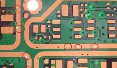
2, Routing of printed circuit board:
The layout of printed conductors shall be as short as possible, especially in high-frequency circuits; The corners of printed wires shall be rounded, and right angles or sharp corners will affect the electrical performance under the condition of high frequency circuit and high wiring density; When two panels are wired, the conductors on both sides should be perpendicular, oblique or curved to avoid parallel to each other to reduce parasitic coupling. The printed conductors used as the input and output of the circuit should avoid adjacent parallel as far as possible to avoid feedback. It is best to add grounding wire between these conductors.
Width of printed conductor: the conductor width should meet the electrical performance requirements and be convenient for production. Its minimum value depends on the withstand current, but the minimum value should not be less than 0.2mm. In high-density and high-precision printed circuits, the conductor width and spacing can generally be 0.3mm; The temperature rise should also be considered in the case of large current. The single panel experiment shows that when the thickness of copper foil is 50 μ m. When the conductor width is 1 ~ 1.5mm and the current is 2a, the temperature rise is very small. Therefore, generally, the conductor with the width of 1 ~ 1.5mm may meet the design requirements without causing temperature rise; The common ground wire of the printed conductor shall be as thick as possible. If possible, use lines greater than 2 ~ 3mm, which is particularly important in the circuit with microprocessor, because when the local line is too thin, due to the change of flowing current, the change of ground potential and the unstable level of microprocessor timing signal, the noise tolerance will be degraded; The 10-10 and 12-12 principles can be applied to the wiring between the IC pins of dip package, that is, when two wires pass between the two pins, the pad diameter can be set to 50mil, the line width and line distance can be 10mil, and when only one wire passes between the two pins, the pad diameter can be set to 64mil, and the line width and line distance can be 12mil.
3, The spacing between printed conductors and adjacent conductors must meet the electrical safety requirements, and the spacing shall be wider as far as possible in order to facilitate operation and production. The minimum spacing shall be at least suitable for the withstand voltage. This voltage generally includes working voltage, additional fluctuation voltage and peak voltage caused by other reasons. If the relevant technical conditions allow a certain degree of metal residues between conductors, the spacing will be reduced. Therefore, the designer should take this factor into account when considering the voltage. When the wiring density is low, the spacing of signal lines can be appropriately increased. The signal lines with great difference between high and low levels should be as short as possible and the spacing should be increased.
4, Shielding and grounding of printed wires the common ground wire of printed wires shall be arranged at the edge of printed circuit board as far as possible. Copper foil should be reserved as much as possible on the printed circuit board as the ground wire. In this way, the shielding effect is better than a long ground wire, the transmission line characteristics and shielding effect will be improved, and the distributed capacitance will be reduced. It is better to form a loop or mesh for the common ground wire of the printed conductor, because when there are many integrated circuits on the same board, especially components with high power consumption, the grounding potential difference is generated due to the graphic limitations, resulting in the reduction of noise tolerance. When the circuit is made, the grounding potential difference is reduced. In addition, the patterns of grounding and power supply should be parallel to the flow direction of data as much as possible, which is the secret of enhancing the ability of noise suppression; Several layers of multilayer printed circuit board can be used as shielding layer, and the power layer and ground wire layer can be regarded as shielding layer. Generally, the ground wire layer and power layer are designed in the inner layer of multilayer printed circuit board, and the signal wire is designed in the inner layer and outer layer.
5, Pad diameter and inner hole size: the inner hole size of the pad must be considered from the element lead diameter and tolerance size, tin lining layer thickness, hole diameter tolerance, hole metallization plating thickness, etc. the inner hole of the pad is generally not less than 0.6mm, because the hole less than 0.6mm is not easy to be processed during die punching, Generally, the metal pin diameter plus 0.2mm is used as the inner hole diameter of the pad. For example, when the metal pin diameter of the resistance is 0.5mm, the inner hole diameter of the pad is 0.7mm, and the pad diameter depends on the inner hole diameter.
1. When the pad diameter is 1.5mm, in order to increase the peeling strength of the pad, long round pads with a length of not less than 1.5mm and a width of 1.5mm can be used. This kind of pad is the most common in the integrated circuit pin pad.
2. The pad diameter beyond the scope of the above table can be selected by the following formula:
Holes with diameter less than 0.4mm: D / D = 0.5 ~ 3 holes with diameter greater than 2mm: D / D = 1.5 ~ 2, where: (D - pad diameter, D - inner hole diameter) VI. other notes related to pads: the distance from the inner hole edge of spot welding pad to the edge of printed circuit board shall be greater than 1mm, so as to avoid pad defect during processing.
Opening of pad: some devices are repaired after wave soldering, but the inner hole of the pad is sealed by tin after wave soldering, so the device cannot be inserted. The solution is to make a small opening on the pad during PCB processing, so that the inner hole will not be sealed during wave soldering and will not affect normal welding.
Pad repair teardrop: when the routing connected to the pad is thin, the connection between the pad and the routing should be designed into a water drop shape. This has the advantage that the pad is not easy to peel, but the routing and pad are not easy to be disconnected.
Adjacent pads shall avoid sharp angles or large areas of copper foil, which will cause difficulty in wave soldering and risk of bridging. Large areas of copper foil will not be easy to weld due to too fast heat dissipation.
7, The large-area copper coating on the large-area copper coated printed circuit board is often used for two functions: one is heat dissipation and the other is shielding to reduce interference. A mistake often made by beginners in designing printed circuit board is that there is no window on the large-area copper coating. Because the adhesive between the substrate of printed circuit board and copper foil is immersed in welding or heated for a long time, It will produce volatile gas, which cannot be eliminated, and the heat is not easy to dissipate, resulting in copper foil expansion and falling off. Therefore, when using large-area copper coating, its open window should be designed into a mesh.
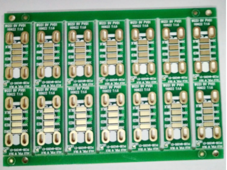
Use of jumper wires: in the design of single-sided printed circuit board, jumper wires are often used when some lines cannot be connected. Among beginners, jumper wires are often random, with long and short, which will bring inconvenience to production. When placing jumper wires, the fewer the types, the better. Usually, there are only 6mm, 8mm and 10mm. Those beyond this range will bring inconvenience to production.
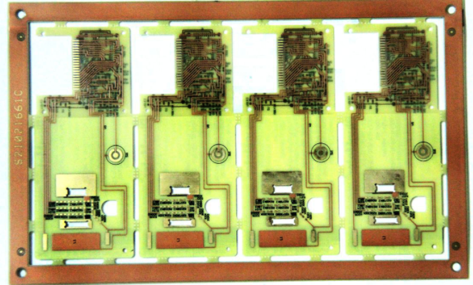
8, Plate and thick printed circuit board are generally made of foil laminate, and copper foil laminate is commonly used. When selecting plates, consideration shall be given to electrical performance, reliability, processing process requirements, economic indicators, etc. common copper-clad laminates include copper-clad phenolic paper laminate, copper-clad epoxy paper laminate, copper-clad epoxy glass cloth laminate, copper-clad epoxy phenolic glass cloth laminate Copper clad PTFE glass cloth laminate and epoxy glass cloth for multilayer printed circuit board. Due to the excellent adhesion between epoxy resin and copper foil, the copper foil has high adhesion strength and working temperature, and can be submerged welded in molten tin at 260 degree Celsius without blistering. Epoxy resin impregnated glass cloth laminate is less affected by moisture. The best material of UHF printed circuit is copper-clad PTFE glass cloth laminate. Flame retardant copper-clad laminate shall also be used on electronic equipment with flame retardant requirements. The principle is that the insulating paper or glass cloth is impregnated with non combustible or flame retardant resin to make the prepared copper-clad phenolic paper laminate, copper-clad epoxy paper laminate, copper-clad epoxy glass cloth laminate and copper-clad epoxy phenolic glass cloth laminate, In addition to the similar properties of similar copper-clad laminates, it also has flame retardancy.
The thickness of the printed circuit board shall be determined according to the function of the printed circuit board, the weight of the components installed, the specification of the socket of the printed circuit board, the overall dimension of the printed circuit board and the mechanical load borne. The total thickness of multilayer printed circuit board and the distribution of thickness between layers shall be selected according to the needs of electrical and structural performance and the standard specification of foil clad board. Common printed circuit board thicknesses are 0.5mm, 1mm, 1.5mm, 2mm, etc.