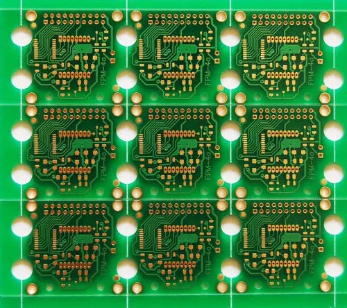
Problems that should be paid attention to when laying copper foil and PCB traces

When laying copper foil, pay attention that the copper foil should be more than 0.5mm away from the edge of the PCB board. When laying copper foil, because the high voltage of the AC wiring part is easy to radiate and discharge, it should be spread as far as possible. Rounded corners; for the sake of uniformity, all copper foils are rounded;
Note: For heavier components, such as radiators (with MOS tube or rectifier tube), common mode inductors, transformers, output INLET or output PIN or terminals, these parts are large, heavy and easy to move, so when laying copper, The copper foil should be as large as possible and should be reinforced with teardrop pads.
Note: Solder mask needs to be added to heat-prone components or high-current copper foil to reduce the impedance so that the copper foil will not be yellowed and the voltage drop will be reduced;
Note: The current carrying capacity of the copper foil is approximately as follows:
The current carrying capacity of 1oz 1mm wide copper foil does not exceed 3.5 amperes of current;
The current carrying capacity of 2oz 1mm wide copper foil does not exceed 7 amperes of current.
Note: The copper foil distance between the high-voltage copper foil and the low-voltage copper foil is about 2KV and the spacing is 2mm; 3KV is about 3.5mm.
Problems that should be paid attention to when PCB wiring;
Note: The AC input part. Under the premise of ensuring the safety distance, the wiring should be as wide as possible; and the wiring should be in the order of the circuit diagram; necking or copper should be used to the X capacitor. In order to have a more comprehensive filtering effect, And it should be as short as possible to reduce its impedance and radiated energy; and it should be as far away as possible from the PWM control part (low voltage part) to avoid interference.
Note that you can’t route wires under the inductor, because passing a wire under the inductor creates an electromagnetic field that changes the electrical properties.
Note: Pay special attention to the SPS PCB Layout, its four current loops:
<1>AC circuit of power switch;
<2>Output rectifier AC circuit;
<3>Input signal source current loop;
<4>Output load current loop.
Make the loop surface as small as possible, and the traces should be as short as possible, especially the two high-current AC loops; the traces of the small signal source current loop should be as short as possible, so that the interference is as small as possible.
Note: In addition, grounding is also very important.Generally speaking, we use single-point grounding, that is, the negative electrode of the input and output capacitors is used as its common point.
The grounding point of the AC loop of the primary current switch should be directly connected to the negative pole of the large capacitor.
The ground wire for the return of the input signal current is also connected to the large capacitor separately.
The Y capacitor should be directly connected to the large input capacitor separately, which is what we often call the single-point grounding method.
Of course, the secondary circuit should also be wired in this way, that is, the output current is the common point for single-point grounding. Note that the ground of 431 should be as short as possible, and it can be directly connected to the negative electrode of the output capacitor.
The above is an introduction to the problems that should be paid attention to when laying copper foil and PCB traces. Ipcb is also provided to PCB manufacturers and PCB manufacturing technology