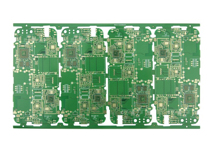
In PCB board design, it is necessary to comprehensively consider the size of the PCB board, pass the current, and select an appropriate line width. PCB copy board, the PCB circuit board industry is often referred to as circuit board copy board, circuit board clone, circuit board copy, PCB clone, PCB reverse design or PCB reverse development.
That is to say, on the premise that there are physical objects of electronic products and circuit boards, reverse analysis of the circuit boards using reverse R&D techniques, and the original product’s PCB files, bill of materials (BOM) files, schematic files and other technical documents and PCB silk screen production documents are restored 1:1.
Then use these technical documents and production documents for PCB manufacturing, component welding, flying probe testing, circuit board debugging, and complete the complete copy of the original circuit board template.

With the continuous development and deepening of the copy board industry, today's PCB copy board concept has been extended to a wider range, and is no longer limited to simple circuit board copy and clone, but also involves the secondary development of products and the development of new products. Research and development.
Then, how to reverse the PCB schematic diagram based on the document diagram or the actual object, and what is the reverse process? What are the details to pay attention to?
Reverse step
1. Record PCB related details
Get a piece of PCB, first record the model, parameter, and position of all the components on the paper, especially the direction of the diode, the triode, and the direction of the IC gap. It is best to use a digital camera to take two photos of the location of the components. Many PCB circuit boards are becoming more and more advanced. Some of the diode transistors on the above are not noticed at all.
2. Scanned image
Remove all components and remove the tin in the PAD hole. Clean the PCB with alcohol and put it into the scanner. When the scanner scans, you need to raise the scanned pixels slightly to get a clearer image.
Then lightly polish the top and bottom layers with water gauze until the copper film is shiny, put them in the scanner, start PHOTOSHOP, and scan the two layers in separately in color.
Note that the PCB must be placed horizontally and vertically in the scanner, otherwise the scanned image cannot be used.
3. Adjust and correct the image
Adjust the contrast and brightness of the canvas to make the part with copper film and the part without copper film have a strong contrast, then turn the second image into black and white, and check whether the lines are clear. If not, repeat this step. If it is clear, save the picture as black and white BMP format files TOP BMP and BOT BMP. If you find any problems with the graphics, you can also use PHOTOSHOP to repair and correct them.
4. Verify the positional coincidence of PAD and VIA
Convert the two BMP format files to PROTEL format files, and transfer them into two layers in PROTEL. For example, the positions of PAD and VIA that have passed through the two layers basically coincide, indicating that the previous steps have been done well. If there is a deviation, then Repeat the third step. Therefore, PCB copying is a work that requires patience, because a small problem will affect the quality and the degree of matching after copying.
5. Draw the layer
Convert the BMP of the TOP layer to the TOP PCB, pay attention to the conversion to the SILK layer, which is the yellow layer, and then you can trace the line on the TOP layer, and place the device according to the drawing in the second step. Delete the SILK layer after drawing. Repeat until all the layers are drawn.
6. TOP PCB and BOT PCB combined picture
Import TOP PCB and BOT PCB in PROTEL and combine them into one picture.
7. Laser printing TOP LAYER, BOTTOM LAYER
Use a laser printer to print the TOP LAYER and BOTTOM LAYER on transparencies (1:1 ratio), put the film on the PCB, and compare whether there are errors. If they are correct, you are done.
8. Test
Test whether the electronic technical performance of the copy board is the same as the original board. If it is the same, it is really done.
Attention to detail
1. Reasonably divide functional areas
When performing the reverse design of the schematic diagram of a good PCB circuit board, a reasonable division of functional areas can help engineers reduce some unnecessary troubles and improve the efficiency of drawing.
Generally speaking, components with the same function on a PCB board are arranged in a concentrated manner, and the division of areas by function can have a convenient and accurate basis when inverting the schematic diagram.
However, the division of this functional area is not arbitrary. It requires engineers to have a certain understanding of electronic circuit related knowledge.
First, find the core component in a certain functional unit, and then according to the wiring connection, you can find other components of the same functional unit along the way to form a functional partition.
The formation of functional partitions is the basis of schematic drawing. In addition, in this process, don't forget to use the serial numbers of the components on the circuit board cleverly, they can help you partition the functions faster.
2. Find the right reference parts
This reference part can also be said to be the main component PCB net city used at the beginning of the schematic drawing. After the reference part is determined, it is drawn according to the pins of these reference parts, which can ensure the accuracy of the schematic drawing to a greater extent. sex.
For engineers, the determination of reference parts is not very complicated. Under normal circumstances, the components that play a major role in the circuit can be selected as reference parts. They are generally larger in size and have more pins, which is convenient for drawing. Such as integrated circuits, transformers, transistors, etc., can all be used as suitable reference components.
3. Correctly distinguish lines and draw wiring reasonably
For the distinction between ground wires, power wires, and signal wires, engineers also need to have relevant power supply knowledge, circuit connection knowledge, PCB wiring knowledge, and so on. The distinction of these lines can be analyzed in terms of the connection of components, the width of the copper foil of the line, and the characteristics of the electronic product itself.
In the wiring drawing, in order to avoid the crossing and interpenetration of lines, a large number of grounding symbols can be used for the grounding line. Various lines can use different colors and different lines to ensure that they are clear and identifiable. For various components, special signs can be used, or even Draw the unit circuits separately, and finally combine them.
4. Master the basic framework and learn from similar schematic diagrams
For some basic electronic circuit frame composition and principle drawing methods, engineers need to be proficient, not only to be able to directly draw some simple and classic unit circuits, but also to form the overall frame of electronic circuits.
On the other hand, don't ignore that the same type of electronic products have a certain similarity in the schematic diagrams. Engineers can use the accumulation of experience and fully learn from similar circuit diagrams to reverse the schematic diagrams of new products.
5. Check and optimize
After the schematic drawing is completed, the reverse design of the PCB schematic can be said to be completed after testing and verification. The nominal value of the components sensitive to the PCB distribution parameters needs to be checked and optimized. According to the PCB file diagram, the schematic diagram is compared and analyzed to ensure that the schematic diagram is completely consistent with the file diagram.