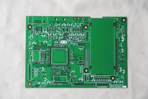
Determine the number of layers of the PCB
The size of the PCB circuit board and the number of wiring layers need to be determined at the beginning of the design. The number of wiring layers and the STack-up method will directly affect the wiring and impedance of the printed lines. The size of the board helps determine the stacking method and the width of the printed line to achieve the desired design effect. At present, the cost difference between multi-layer boards is very small, and it is better to use more circuit layers and make the copper distribution evenly at the beginning of the design.

2. Design rules and restrictions
To successfully complete the wiring task, wiring tools need to work under the correct rules and restrictions. To classify all signal lines with special requirements, each signal class should have a priority. The higher the priority, the stricter the rules. The rules involve the width of the printed lines, the maximum number of vias, the degree of parallelism, the mutual influence between the signal lines, and the limitation of layers. These rules have a great influence on the performance of the wiring tool. Careful consideration of design requirements is an important step for successful wiring.
3. Layout of components
In the optimal assembly process, design for manufacturability (DFM) rules impose restrictions on component layout. If the assembly department allows components to move, the circuit can be appropriately optimized.
1. In the PCB layout, the power supply decoupling circuit should be designed near the relevant circuits, rather than placed in the power supply part, otherwise it will affect the bypass effect, and pulsating current will flow on the power line and the ground line, causing crosstalk;
2. For the power supply direction inside the circuit, power should be supplied from the final stage to the previous stage, and the power supply filter capacitor of this part should be arranged near the final stage;
3. For some main current channels, such as disconnecting or measuring current during debugging and testing, current gaps should be arranged on the printed wires during layout. In addition, it should be noted that the regulated power supply should be arranged on a separate printed circuit board as much as possible during the layout. When the power supply and the circuit share a p rinted PCB circuit board, in the layout, it should be avoided that the stabilized power supply and the PCB circuit components are mixed or the power supply and the circuit share the ground wire. Because this kind of wiring is not only easy to produce interference, but also unable to disconnect the load during maintenance, only part of the printed wires can be cut at that time, thereby damaging the printed board.