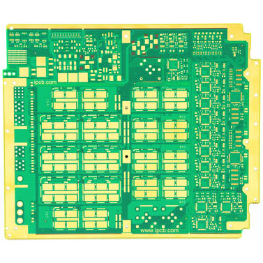
The frequency of the signal processed by the circuit is high enough so that the impedance of the transmission line at this frequency is sufficient to affect the signal. A circuit that works at this frequency is called a high-speed circuit PCB.

1. What is a high-speed circuit PCB
It is generally believed that if the frequency of a digital logic circuit reaches or exceeds 45MHZ~50MHZ, and the circuit working above this frequency has already accounted for a certain share of the entire electronic system (for example, 1/3), it is called a high-speed circuit. In fact, the harmonic frequency of the signal edge is higher than the frequency of the signal itself. It is the rising and falling edges of the signal (or signal jump) that cause unexpected results of signal transmission. Therefore, it is generally agreed that if the line propagation delay is greater than 1/2 of the rise time of the digital signal driving end, such signals are considered to be high-speed signals and produce transmission line effects.
The transmission of the signal occurs at the instant when the signal state changes, such as the rise or fall time. The signal passes a fixed period of time from the driving end to the receiving end. If the transmission time is less than 1/2 of the rise or fall time, the reflected signal from the receiving end will reach the driving end before the signal changes state. Conversely, the reflected signal will reach the drive end after the signal changes state. If the reflected signal is strong, the superimposed waveform may change the logic state.
2. Determination of high-speed signals
Above we have defined the preconditions for the occurrence of transmission line effects, but how do we know whether the line delay is greater than 1/2 the signal rise time of the drive end? Generally, the typical value of the signal rise time can be given in the device manual, and the signal propagation time is determined by the actual wiring length in the PCB design. The following figure shows the corresponding relationship between the signal rise time and the allowable wiring length (delay).
The delay per unit inch on the PCB is 0.167ns. However, if there are many vias, many device pins, and many constraints set on the network cable, the delay will increase. Generally, the signal rise time of high-speed logic devices is about 0.2ns. If there are GaAs chips on the board, the maximum wiring length is 7.62mm.
Let Tr be the signal rise time and Tpd be the signal line propagation delay. If Tr≥4Tpd, the signal falls in a safe area. If 2Tpd≥Tr≥4Tpd, the signal falls in the uncertainty region. If Tr≤2Tpd, the signal falls in the problem area. For signals falling in uncertain areas and problem areas, high-speed wiring methods should be used.
Simple layout design can be realized by hand, and complex layout design needs to be realized with the help of computer-aided design (CAD). Excellent layout design can save production cost and achieve good circuit performance and heat dissipation performance.
The above is the introduction of high-speed circuit PCBs, Ipcb also provides PCB manufacturers and PCB manufacturing technology