1 Surface tension
Everyone is familiar with the surface tension of water. This force keeps the cold water droplets on the grease-coated metal plate in a spherical shape. This is because in this example, the adhesion force that makes the liquid on the solid surface tend to spread is less than its cohesive force. Wash with warm water and detergent to reduce its surface tension. The water will infiltrate the grease-coated metal plate and flow outward to form a thin layer. This will happen if the adhesion force is greater than the cohesion force.

The cohesion of tin-lead solder is even greater than that of water, making the solder spheres to minimize its surface area (under the same volume, the sphere has the smallest surface area compared with other geometric shapes to meet the needs of the lowest energy state) . The effect of the flux is similar to that of the cleaner on the grease-coated metal plate. In addition, the surface tension is highly dependent on the cleanliness and temperature of the surface. Only when the adhesion energy is much greater than the surface energy (cohesion) can ideal adhesion occur. tin.
2 Wetting effect
When the hot liquid solder dissolves and penetrates to the surface of the metal to be welded, it is called metal dip tin or metal dip tin. The molecules of the mixture of solder and copper form a new alloy partly made of copper and partly soldered. This solvent action is called tin dip, which forms an intermolecular bond between each part to form a metal alloy eutectic. The formation of good intermolecular bonds is the core of the welding process, which determines the strength and quality of the welding joint. Only the surface of the copper is not polluted, and there is no oxide film formed by exposure to the air to be wetted with tin, and the solder and the working surface need to reach an appropriate temperature.
3 Dip tin corner
When the eutectic point temperature of solder is about 35°C higher, when a drop of solder is placed on a hot flux-coated surface, a meniscus is formed. To a certain extent, the ability of the metal surface to dip tin It can be evaluated by the shape of the meniscus. If the solder meniscus has a distinct undercut edge, shaped like a drop of water on a greased metal plate, or even tends to be spherical, the metal is not weldable. Only the meniscus stretched to a size less than 30. It has good weldability at a small angle.
4 Generation of metal alloy alloys
The intermetallic bond between copper and tin forms crystal grains. The shape and size of the crystal grains depend on the duration and strength of the temperature during soldering. Less heat during welding can form a fine crystalline structure, forming an excellent welding point with the best strength. Too long reaction time, whether due to too long welding time or too high temperature or both, will result in a rough crystalline structure, which is gravel and brittle, and has low shear strength.
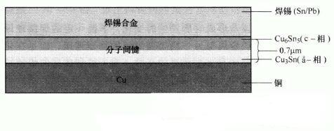
Copper is used as the metal substrate and tin-lead as the solder alloy. Lead and copper will not form any metal alloys. However, tin can penetrate into the copper, and the intermolecular bond between tin and copper forms a metal on the joint surface of the solder and the metal. Alloy eutectic Cu3Sn and Cu6Sn5, as shown in the figure.

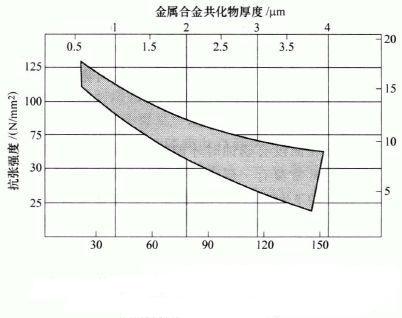
The metal alloy layer (n phase + epsilon phase) must be very thin. In laser welding, the thickness of the metal alloy layer is on the order of 0.1mm. In wave soldering and manual soldering, the thickness of the intermetallic bond in good solder joints is mostly more than 0.5μm. Since the shear strength of the solder joint decreases with the increase of the thickness of the metal alloy layer, it is often tried to keep the thickness of the metal alloy layer below 1 μm, which can be achieved by making the welding time as short as possible.
The thickness of the metal alloy eutectic layer depends on the temperature and time to form the solder joints. Ideally, the soldering should be completed within 220 ”t about 2s. Under this condition, the chemical diffusion reaction of copper and tin will produce an appropriate amount of The thickness of the metal alloy bonding materials Cu3Sn and Cu6Sn5 is about 0.5μm. Insufficient intermetallic bonds are common in cold solder joints or solder joints that are not raised to the proper temperature during welding, which may cause the welding surface to be cut off. On the contrary, a metal alloy layer that is too thick is common in solder joints that are overheated or soldered for too long, which will result in very weak tensile strength of the solder joints, as shown in the figure.

The above is the introduction of PCB board soldering methods.