In any electronic system, the interference of the interference source to the system is nothing more than two ways: one is transmission through conductors, and the other is coupling through space through electromagnetic radiation. In low-frequency systems, it is mainly the first path. In high-frequency systems, a considerable part of the cause of interference is transmission through conductors. The more obvious one is that the noise generated by IC interferes with the entire system through power and ground. Therefore, the integrity of the power supply or the quality of the power supply is of vital importance to the anti-interference ability of the entire system. Power integrity is actually a part of signal integrity, but considering the importance of power to all systems, it is listed separately here. It should be stated that it is not easy to do this in an actual system. There will always be noises of different frequencies in the system. In the circuit design and PCB layout and routing, it is only trying to reduce the noise of various frequencies, thereby improving the overall performance of the anti-noise of the system. At the same time, in a complex system, reducing the noise of the system is not to change the value of one or two capacitors, but to pay attention to the accumulation of power supply filtering effects. In the hardware design of mobile phones, there are dedicated PMUs to manage and supply power to each module, but the PMUs are all from VBAT. It is impossible to imagine that if the power supply of a sensitive audio op amp is not filtered and is directly taken from VBAT, or, like the circuit that supplies power to SDRAM, it is not filtered, and the switching noise of this part of the digital circuit is allowed to pollute the entire VBAT. What are the consequences?

If enough attention is paid to the integrity of the power supply, this part is relatively easy to deal with after combining the modularity mentioned above and careful analysis of each module. The usual rules for IC power supply VCC are generally handled by bypass capacitors and decoupling capacitors, and try to keep these capacitors close to the power input of the IC when laying out the board. If you are in a demanding system, you can also use an LCCL circuit for different sensitive frequencies (connect an inductor or a magnetic bead in series, and an electrolytic capacitor, and a ceramic capacitor, and then a small inductor in series. The specific value needs to follow The corresponding frequency is determined) filtering. I used to make a complicated system. Because there is no bypass capacitor on the core power supply of the system's DEMODULATOR, the DEMODULATOR's bit error rate after demodulation is unbearable. For the processing of various GNDs in the system, it is generally required to analyze the return path of the current. The current has the property of always selecting the return path with the least impedance. This is a core principle, which can be understood by the fact that there is a pattern of "copper laying" in PCB wiring. "Paving copper" is often used on the network GND. All digital signals can be abstracted into a most basic gate-level circuit. GND is also a part of the signal return path. GND is to make the total impedance on the signal path smaller by "laying copper". "Nearby grounding" and "minimizing ground impedance" are also based on such considerations.
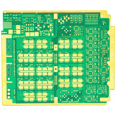
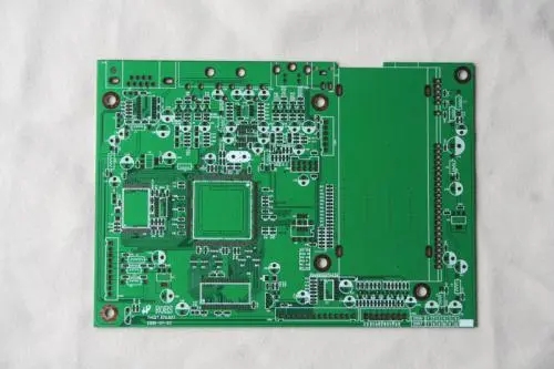
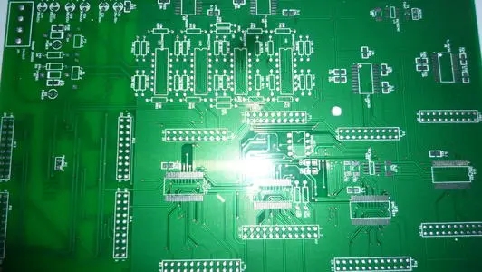
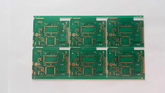
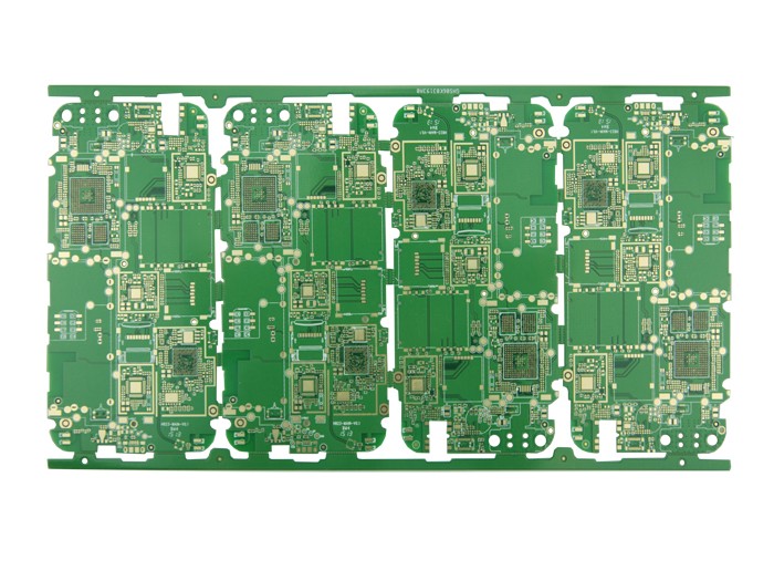
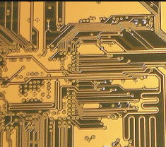
The above is an introduction to the processing of power and ground wires in the layout and routing. Ipcb is also provided to PCB manufacturer and PCB manufacturing technology