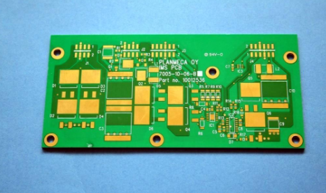
The wiring is mainly carried out according to the following principles:

1. . Under normal circumstances, the power line and ground line should be wired first to ensure the electrical performance of the circuit board. As far as conditions allow, widen the power supply as much as possible. The width of the ground wire, preferably the ground wire is wider than the power wire, their relationship is: ground wire>power wire>signal wire, usually the signal wire width is: 0.2~0.3mm, the smallest width can reach 0.05~0.07mm, power supply The line is generally 1.2 ~ 2.5mm. For the PCB of the digital circuit, a wide ground wire can be used to form a loop, that is, to form a ground net to use (the ground of the analog circuit cannot be used in this way)
2. . Wire the lines with strict requirements (such as high-frequency lines) in advance, and the edges of the input end and the output end should be avoided adjacent and parallel to avoid reflection interference. If necessary, ground wire should be added for isolation, and the wiring of two adjacent layers should be perpendicular to each other. Parasitic coupling is easy to occur in parallel.
3. . The housing of the oscillator is grounded, and the clock line should be as short as possible, and it should not be drawn everywhere. Below the clock oscillation circuit. The area of the special high-speed logic circuit should be enlarged, and other signal lines should not be used to make the surrounding electric field approach zero;
4. . Use 45o polyline wiring as much as possible, and 90o polyline should not be used to reduce the radiation of high-frequency signals; (highly demanding lines should also use double arc lines)
5. . Do not form a loop on any signal line. If it is unavoidable, the loop should be as small as possible; the signal line’s vias should be as few as possible;
6. . The key line should be as short and thick as possible, and protective ground should be added on both sides.
7. . When transmitting sensitive signals and noisy field band signals through flat cables, they should be led out in the way of "ground wire-signal-ground wire".
8. . Key signals should be reserved for testing points to facilitate production and maintenance testing
9. . After the schematic wiring is completed, the wiring should be optimized; at the same time, after the preliminary network inspection and DRC inspection are correct, the unwiring area is filled with ground wire, and a large area of copper layer is used as the ground wire. All places used are connected to the ground as a ground wire. Or it can be made into a multilayer board, and the power supply and ground wires occupy one layer each.
The above is the introduction of PCB board wiring mainly according to the following principles. Ipcb is also provided to PCB manufacturers and PCB manufacturing technology.