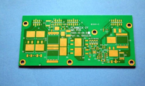
Printed wires should take the shortest route between components under the constraints of the specified wiring rules. Limit the coupling between parallel wires as much as possible. Good design requires the minimum number of wiring layers, and also requires the widest wire and the largest pad size corresponding to the required packaging density. Because rounded corners and smooth inner corners may avoid some electrical and mechanical problems that may occur, sharp corners and sharp corners in the wire should be avoided.

PCB board width and thickness
The figure shows the current-carrying capacity of etched copper wires on rigid printed boards. For 1oz and 2oz wires, taking into account the etching method, the normal variation of copper foil thickness and the temperature difference, it is allowed to reduce the nominal value by 10% (in terms of load current); for the printed board assembly coated with a protective layer (The thickness of the base material is less than 0.032 inches, and the thickness of the copper foil is more than 3 ounces), the components are reduced by 15%; for the printed board that has been dipped, it is allowed to reduce by 30%.
PCB wire spacing
The minimum spacing of wires must be determined to eliminate voltage breakdown or arcing between adjacent wires. The spacing is variable, it mainly depends on the following factors:
1) Peak voltage between adjacent wires.
2) Atmospheric pressure (maximum working altitude).
3) The coating layer used.
4) Capacitive coupling parameters.
Critical impedance components or high-frequency components are generally placed very close to reduce the critical stage delay. Transformers and inductive components should be isolated to prevent coupling; inductive signal wires should be laid orthogonally at right angles; components that generate any electrical noise due to magnetic field movement should be isolated or rigidly installed to prevent excessive vibration.
The above is the introduction of PCB routing and positioning. Ipcb is also provided to PCB manufacturers and PCB manufacturing technology.