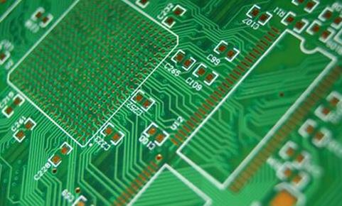
For the noise on the PCB board, when it is found that electromagnetic interference occurs in the digital circuit, the main reason is that the obvious noise voltage can be observed on the power line and the ground line with an oscilloscope. Although many people can conclude that these noises are the cause of electromagnetic interference problems in circuits, they do not know how to solve them. In order to achieve the purpose of eliminating noise, it is necessary to first understand how these noises are generated.

1. Noise on the power line
For a typical gate circuit output stage, when the output is high, Q3 is turned on and Q4 is turned off; when the output is low, Q3 is turned off and Q4 is turned on. Both of these states create a high impedance between the power supply and ground, which limits the current flow from the power supply. When the state changes, Q3 and Q4 are temporarily turned on at the same time. At this time, a short-term low impedance is formed between the power supply and the ground, resulting in a peak current of 30-100 mA. When the gate output level changes from low to high, the power supply not only maintains the output current, but also charges the parasitic capacitance to saturate this current peak. Since the power line has different degrees of inductance, when the current changes suddenly, an induced voltage is generated. This is the observed noise on the power line. A brief dip in voltage occurs due to power line impedance.
2. Noise on the ground
When the above-mentioned peak current is generated, current will also flow on the ground wire, especially when the output level changes from high to low, the parasitic capacitance is discharged, and the peak current on the ground wire is larger. Since the ground wire always has different degrees of inductance, voltage will also be induced, which results in ground wire noise. Noise on the ground and power lines will not only make the circuit run poorly, but also generate strong electromagnetic radiation. "Icc" (current on power supply): The amplitude is different at different output states. When stable, the current is also stable. When the output changes from low to high, it is short-circuited instantaneously, the current increases, and the parasitic capacitance is charged at the same time, and the current is larger; when the output level changes from high to low, it is short-circuited instantaneously, and the current increases, but the parasitic capacitance is not charged, so The current is smaller than when the output level changes from low to high. Voltage "Vcc" (voltage on power supply): When Icc changes abruptly, the inductance L of the power line will generate an induced voltage "Ldi/dt". "Ig" (ground current): The current on the power line and the discharge of parasitic capacitances in the circuit. The output is stable and the current is stable. When the output level changes from low to high, there is an instant short circuit and the current increases. When the output level changes from high to low, there is an instantaneous short circuit, the current increases, and the parasitic capacitance discharges at the same time, and the current peak value is larger than that when the output level changes from low to high. "Vg" (ground wire voltage): When the "Ig" changes suddenly, the inductance L of the ground wire will have an induced voltage "Ldi/dt".
Power line, ground line noise voltage waveform
Although the method to solve the noise voltage of the ground line can set the power line grid on the circuit board to reduce the inductance, but it takes up a lot of wiring space. In order to reduce the inductance of the power supply line, the following methods can be adopted: use the energy storage capacitor, whose function is to supply the chip with the large current required when the output state of the circuit changes, thus reducing the induced noise voltage and avoiding the Current mutation. Storage capacitors limit current changes to a small range and reduce radiation, so add some storage capacitors when using power line grids or power line planes (power systems have small inductance) on the circuit board. Because the energy storage capacitor provides transient high energy for the chip, it should be as close to the chip as possible in the wiring stage, that is, the area of the power supply circuit of the energy storage capacitor should be as small as possible, or the space between the energy storage capacitor and the chip power supply terminal and the ground terminal should be kept as small as possible. The traces should be as short as possible. The length of the trace between the chip and the energy storage capacitor is the length of the chip's own pins plus the length of the circuit board trace. Therefore, in order to reduce the total length of these two parts, it is necessary to select chips with power pins and ground pins close to each other, and avoid using chip mounts, surface-mounted chips, etc. In addition, after the discharge of the energy storage capacitor of each chip, the charge must be replenished in time to prepare for the next discharge. In order to reduce the disturbance to the power supply system, the charge can be provided by a capacitor called secondary energy storage. When there are few chips on the circuit board, a secondary energy storage capacitor can be installed at the entrance of the power line. The capacity of the secondary energy storage capacitor should be more than 5 times the total capacity of the chip energy storage capacitor. If there are many chips on the circuit board, set a secondary energy storage capacitor every 5 to 10 chips. Tantalum capacitors should be used for this capacitor, and the series inductance should be as small as possible. Do not use aluminum electrolytic capacitors to cause internal inductance on PCB board.