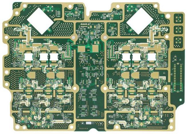
Multilayer circuit board stack structure
Before designing a multilayer circuit board, the designer needs to first consider the size of the circuit, the size of the PCB circuit board, and electromagnetic compatibility (EMC) requirements to determine the circuit board structure used, that is, decide whether to use 4 layers circuit board, 6 layers circuit board or more circuit board.
After determining the number of layers, determine the placement position of the inner electric layer and how to distribute different signals on these layers. this is the problem of selecting a multilayer PCB stack structure. The stack structure is an important factor affecting the EMC performance of PCB circuit boards. It is an important means to suppress electromagnetic interference. This section will introduce the related contents of the multilayer circuit board stack structure.
Principle of layer selection and superposition.
Many factors need to be considered to determine the stacking structure of multilayer PCB Boards. In terms of cabling, the more layers, the better for cabling, However, the cost and difficulty of plate making will also increase. For manufacturers, whether the laminated structure is symmetrical or not is PCB manufacturing, therefore, the selection of layers needs to consider the needs of all aspects to achieve the best balance. Experienced designers, after completing the pre-layout of components, will focus on the wiring bottleneck of PCB analysis. Analyze the wiring density of the circuit board with other EDA tools; Re-synthesize signal lines with special wiring requirements, such as differential. The number and type of lines and sensitive signal lines determine the number of signal layers; Then, according to the type, isolation, and anti-interference of power supply determine the number of inner electric layers. In this way, the number of layers of the whole circuit board is basically determined.
After determining the number of layers of the circuit board, the next work is to arrange the placement order of each layer of circuits reasonably. In this step, There are two main factors to consider.
1. Distribution of special signal layers.
2. Distribution of power supply layer and stratum.
If there are more layers in the circuit board, there will be more types of arrangement and combination of special signal layer, stratum and power supply layer. How to determine.It is more difficult to determine which combination mode is optimal, but the general principles are as follows.

1. The signal layer should be adjacent to an internal electric layer (internal power supply/stratum), and the large copper film of the internal electric layer is used to lift the signal layer for shielding. The internal power layer and stratum should be closely coupled, that is, the medium thickness between the internal power layer and stratum.
A smaller value should be taken to increase the capacitance between the power supply layer and the formation and increase the resonant frequency. Between the internal power layer and stratum. The media thickness of the can is set in Protel's Layer Stack Manager. Select the Design command. The system pops up the layer stack manager dialog box. Double-click the Prepreg file with the mouse. This allows you to change the thickness of the insulation layer in the Thickness option of the dialog box. If the potential difference between the power supply and the ground wire is small, a smaller insulation layer thickness, such as 5mil, can be used(0.127mm).
3. The high-speed Circuit board signal transmission layer in the circuit should be the signal intermediate layer and sandwiched between two inner electric layers. In this way, The copper film of the electrical layer can provide electromagnetic shielding for high-speed signal transmission, and can also effectively limit the radiation of high-speed circuit board signals to two. There is no external interference between the inner electric layers.
4. Avoid two signal layers being directly adjacent. It is easy to introduce crosstalk between adjacent signal layers, which leads to circuit functional failure. Adding a ground plane between two signal layers can effectively avoid crosstalk.
5. Multiple grounded inner electric layers can effectively reduce the grounding impedance. For example, A signal layer and B signal layer adopt their own single. The unique ground plane can effectively reduce common mode interference.
6. Considering the symmetry of the layer structure.
This is the related content of the multilayer circuit stack structure to the PCB circuit board.