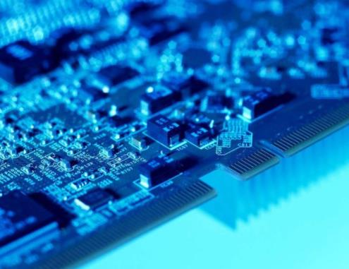
The development of modern electronic science and technology is becoming more and more vigorous. The single-layer or even double-layer PCB board can no longer meet the needs of scientific and technological personnel, and everyone has begun to pursue higher and more precise PCB boards. In the manufacturing process of PCB, lamination is a very important process. A printed circuit board (PCB) is a structure for connecting and supporting electronic components. The PCB board has a conductive path through which different components can be connected to the whole board. These channels are etched from copper sheets. To ensure that the copper layer does not conduct signals or currents, please laminate it into the substrate.

Type of PCB board laminating program
The following are commonly used PCB laminating processes, depending on the type of PCB used:
1. Multilayer PCB board: A circuit board composed of various layers is called a multilayer PCB board. These layers can be thin etched plates or routing layers. In both cases, they are bonded together by lamination. For lamination, the inner layer of the PCB board is subjected to extreme temperature (375o F) and pressure (275 to 400 psi). Perform this procedure when laminating with photosensitive dry resist. After that, allow the PCB to cure at high temperatures. Finally, slowly release the pressure and slowly cool the laminate.
2. Double-sided PCB board: Although the manufacturing of double-sided PCB boards is different from other types of PCB boards, the laminating process is very similar. The photosensitive dry resist layer is used for laminating PCB boards. As described in multilayer PCB, the process is carried out under extreme temperature and pressure.
3. Sequential lamination: If the PCB board contains two or more subsets, the sequential lamination technique is used. Subsets of multilayer PCB boards are created in a separate process. Thereafter, a dielectric material is inserted between each pair of subsets. The standard manufacturing procedure is followed by this process.
4. Teflon PCB(PTFE) microwave laminate: PTFE microwave laminate is one of the most commonly used laminates for PCB lamination. The reason is that it has a consistent dielectric constant, extremely low electrical loss and strict thickness tolerance. These features are ideal for printed circuit boards for applications that include RF. CTFE (Chlorotrifluoroethylene) thermoplastic film is a commonly used material for PTFE lamination.
When making PCB proofing, customers often put forward higher requirements on the manufacturer's delivery date, ability to handle complex samples, and product quality. What problems do you usually need to pay attention to in the PCB proofing process?
1. Pay attention to the number of samples
Before large-scale mass production, enterprises often need to make a batch of PCB templates for testing, which actually accounts for a certain cost of the enterprise. Especially when the enterprise is large in size and produces many types of PCB boards, the cost of PCB proofing and testing is also very considerable. From this point of view, enterprises should pay attention to the number of samples during PCB proofing.
2. To confirm the device packaging
Welding chips with specific functions on the circuit board and packaging them with shielding cover is a process in the circuit board manufacturing process. In the process of PCB proofing, the entrusting party should pay great attention to whether the internal chips and electronic components are wrongly soldered during packaging, so as to ensure the quality of PCB proofing, and then normal verification functions and subsequent further large-scale production can be achieved.
3. Comprehensive electrical inspection is required
After PCB proofing, the enterprise should conduct a comprehensive electrical inspection to ensure that every function and every detail of the PCB are checked. This is the significance of PCB proofing, and also the guarantee of whether the subsequent PCB can be put into mass production and ensure an extremely low defective rate. To conduct a comprehensive electrical inspection, it is recommended that the entrusting party cooperate with the sampling party to carry out a more rigorous test method. Of course, there are still some signal integrity layouts that need to be paid attention to and solved by both parties, but generally speaking, the problems that need to be paid attention to in PCB proofing are roughly the above items. Although there are many questions about what PCB board proofing means in the market, as an insider, doing a comprehensive investigation and testing of the above issues is the basis for ensuring the quality of PCB board samples and transforming them into subsequent mass production. PCB board proofing must be taken seriously.