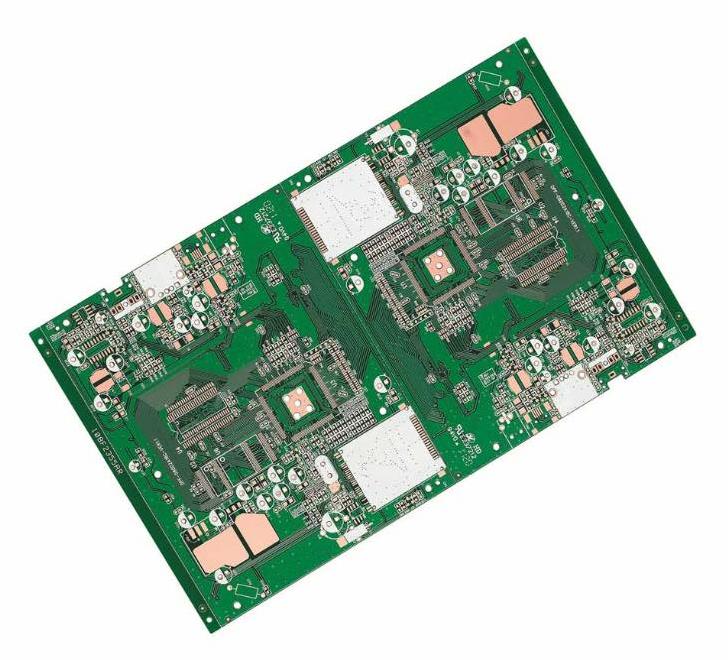
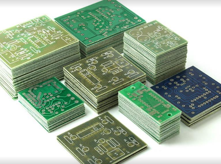
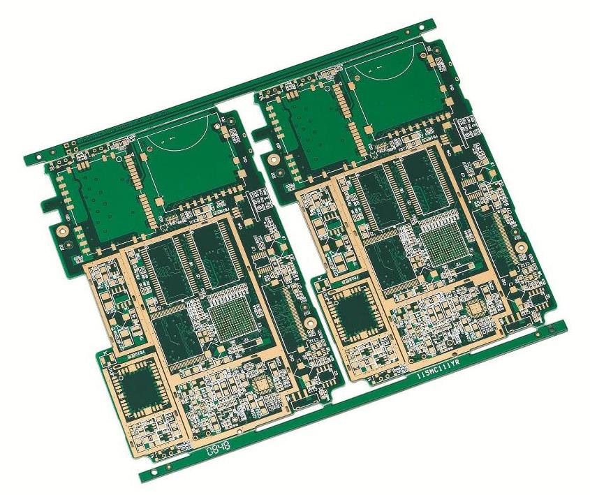
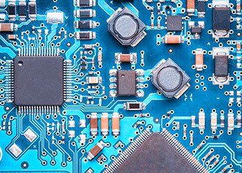
With the development of PCB design and the rapid increase of frequency, in addition to the design of high-frequency PCB, many interferences are inconsistent. With the increase of frequency, the miniaturization and cost reduction of PCB become more obvious.
These disturbances become more and more complex. The current research has concluded that there are four main types of interference: voltage noise, transmission line interference, coupling and electromagnetic interference. In this paper, we analyze various interference problems of high-frequency circuit board, and propose effective solutions combined with practice.
In the high-frequency PCB circuit of power supply noise, power supply noise is particularly important for high-frequency PCB signals. Therefore, the power supply is required to have low noise first. Here, clean ground is as important as clean electricity. Why? Obviously, the power supply has a certain impedance, and the impedance is distributed on the whole power supply, so the noise is also superimposed on the power supply.
Then, we should reduce the impedance of the power supply as much as possible, so it is better to have a proprietary power layer and ground plane. In high-frequency circuit design, the power supply is designed hierarchically, which is much better than the bus form in most cases, so the loop can always follow the path with the minimum impedance.In addition, the power board must provide a signal loop for all generated and received signals on the high-frequency PCB, thereby minimizing the signal loop and reducing noise, which is usually ignored by low-frequency circuit designers.
Pay attention to the through-hole on the board: the through-hole must be etched into the opening on the power layer to leave space for the through-hole to pass through. If the power layer is too large, the signal loop will be affected, the signal will be forced to bypass, the loop area will increase, and the noise will also increase. At the same time, if some signal lines are concentrated near the opening and share the loop, the common impedance will cause crosstalk.
The cable needs to be grounded sufficiently: each signal needs its own proprietary signal loop, and the loop area of the signal and loop should be as small as possible, that is, the signal is parallel to the loop.
Analog and digital power supplies should be placed separately: high-frequency equipment is usually very sensitive to digital noise, so they should be separated and connected together at the power inlet. If the signal goes through both analog and digital crossovers, it may be at the signal crossover. Place a ring to reduce the ring area.

Power line coupling: When the AC or DC power line is subject to electromagnetic interference, the power line will transmit the interference to other devices. There are several ways to eliminate crosstalk in PCB design: the size of both crosstalk increases with the increase of load impedance, so signal lines sensitive to interference caused by crosstalk should be transmitted correctly.
The capacitance crosstalk can be effectively reduced by increasing the distance between signal lines as much as possible. Perform ground plane management and space between wiring (for example, separate active signal lines from ground wires, especially between signal lines with state jump and further increase of ground distance), and set lead inductance to decrease.
Inserting grounding wires between adjacent signal lines can also effectively reduce capacitive crosstalk, which requires every 1/4 wavelength to enter the grounding plane.
For induced crosstalk, the loop area shall be minimized and eliminated as much as possible. Avoid signal sharing loops. Focus on signal integrity: designers need to achieve termination during welding to solve signal integrity problems.
Designers using this method can focus on the microstrip length of the shielding copper foil to achieve good signal integrity. For systems that use dense connectors in communication structures, designers can use a single PCB design for termination.
With the increase of speed, EMI will become more and more serious and show itself in many aspects (such as the electromagnetic interference at the interconnection). The high-speed device is particularly sensitive to this, so it will receive high-frequency PCB error signals. Low speed devices ignore such error signals.
There are several methods to eliminate electromagnetic interference in PCB design:
Reduce loops: Each loop is equivalent to an antenna, so we need to minimize the number of loops, loop area, and loop antenna effect. Ensure that the signal has only one loop at any two points, avoid artificial loops, and use the power plane as much as possible.
Filtering: You can use filtering on power lines and signal lines to reduce EMI. There are three methods: decoupling capacitors, EMI filters, and magnetic components. The EMI filter is shown in the figure.Due to the length of the problem and many articles on shielding, we will not specifically describe how to reduce the speed of high-frequency equipment as much as possible. Increasing the dielectric constant of the PCB board can prevent the high-frequency PCB of the transmission line near the board from radiating outward.
Increasing the thickness of PCB board and minimizing the thickness of microstrip line can prevent the overflow of electromagnetic line and also prevent radiation.In the discussion, we can conclude that in the design of high-frequency PCB, we should follow the following principles: unity and stability of power supply and ground. Careful wiring and proper termination eliminate reflections. Careful consideration of cabling and proper termination can reduce capacitive and inductive crosstalk. In order to meet high-frequency PCB requirements, noise suppression is required.