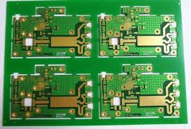
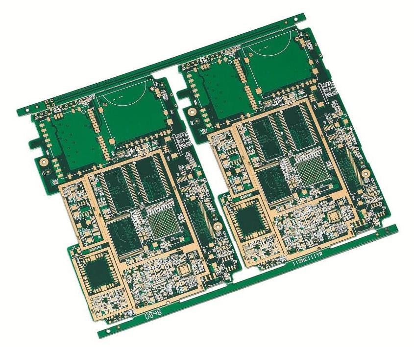
Cadence tool includes PCB assembly and PCB design components. From now on, learn PCB design components and compare them with AlTIum (Protel). Cadence PCB assemblyuse discrete tools, which is different from Altium. With 16. x as the standard, there are nearly 10 components.
1. Consider PCB assembly footprints
Here, we refer to the layout stage, in which the pad pattern and space occupation decisions need to be considered. In fact, you should consider the decision of the component footprint throughout the drawing phase of the schematic involved. It is also important to note that the coverage area will include the mechanical components of the parts involved as well as electrical pad connections.
In other words, it will involve pins fixed to the printed circuit board and the body contour of the PCB assembly. Therefore, when deciding which component to choose, consider any packaging or enclosure limitations that may be encountered when evaluating the bottom and top of the final printed circuit board.
For example, polarized capacitors and other such components often have high gap limits and need to be considered as part of the unit selection process. When you begin to design the layout, you may need to draw a basic board outline shape, and then place the connectors or other such key placed components that you want to use. In this way, you will be able to create a virtual rendering of PCBs that is not only fast but also does not require any wiring.
The resulting visualization can then be used to create a very accurate visual representation of the height and relative position of components and slabs. In this way, once the PCB is assembled, you can ensure that all involved parts (such as mechanical frame, chassis and plastic) can be put into the package.

2. Prepare for change
The selection of components may change through various designs. The design process is constantly changing, and you should consider which components will use surface plating technology and which components will be plated through holes. The whole planning process of PCB design can be simplified by pre selecting the route to be taken. Before deciding which PCB assembly to use, we must carefully consider power consumption, component area density, component cost and availability.
In general, surface mount technology components are easier to access and obtain than their counterparts in electroplated through-hole components. In addition, at least from the manufacturing point of view, they tend to be cheaper than their electroplated through-hole components.
Interestingly, for medium and small prototyping tasks, it is recommended to use larger through-hole parts or surface mount technology components to facilitate better access to signals and pads during debugging and troubleshooting tasks, and they can also simplify the manual welding process. It is also important to note that if you cannot obtain a specific footprint in the database, you can design a custom footprint from the tool.
3. Implement good grounding practices
The design you include should have a sufficient number of ground planes and bypass capacitors. If an IC is used, ensure that an appropriate number of decoupling capacitors are used near the power supply at the ground plane or other such locations.
Obviously, the capacitor size you choose will largely depend on the frequency involved and the capacitor technology and application type implemented. In conclusion, it is very important to follow good grounding specifications, because this will enable your printed circuit board to have optimized magnetization and excellent electromagnetic compatibility.
4. Assign virtual part footprints correctly
It is strongly recommended that you run a bill of materials or BOM to check for any virtual PCB assembly. There is no encapsulation associated with virtual components, and they will not be transferred to the layout phase. By creating a bill of materials, you can evaluate all virtual parts in the design.
On the input side, you should only input ground and power signals, because they are actually virtual components that are specifically handled in a schematic environment rather than a layout environment. In summary, PCB assembly found in the virtual part should always be replaced by components that actually have footsteps, unless they are used only for simulation reasons.
5. Check the spare door
In order to prevent the input from floating, PCB design the input of all standby doors shall be correctly fixed on the signal. Unfortunately, PCB assembly can sometimes be omitted or forgotten, so you should take the time to check all forgotten doors or spare doors to ensure that any unconnected inputs can be properly secured if necessary. Although rare, floating inputs can sometimes cause serious problems, such as causing the entire system to fail to operate as expected.