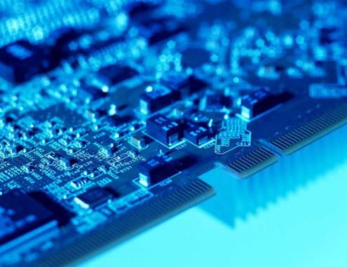
The main reason for the reserved process edge in PCB board production is that the SMT mounter track is used to clamp the circuit board and flow through the mounter. Therefore, when components too close to the track edge are absorbed by the SMT mounter nozzle and mounted on the circuit board, the collision phenomenon occurs and the production cannot be completed. Therefore, in the process of PCB assembly production, the process edge is generally added in order to consider the subsequent patches and plug-ins. So, what are the advantages of reserving process edges for PCB production?

The reserved process edge is to assist the patch plug-in to weld the added parts on both sides or four sides of the PCB board, which are not part of the PCB board and can be removed after the manufacturing and production of PCB board A. The reserved process edge for PCB production will consume more boards and increase PCB production cost. Therefore, when designing PCB process edges, it is necessary to balance economy and manufacturability. For some special PCB, the original PCB with 2 or 4 process edges can be greatly simplified by PCB assembly. The track width of SMT mounter shall be fully considered when designing the splicing method for SMT chip mounting processing. For the splicing of more than 350mm in width, it is necessary to communicate with the process engineer of SMT supplier. The flatness of PCB production process edge is also an important part of PCB production. When removing the process edge of PCB production, it is necessary to ensure that the process edge is flat. Especially for PCB with high assembly accuracy requirements, any uneven burr will lead to the offset of the installation hole position, which will bring great trouble to subsequent PCB assembly.
To make a complete PCB board, it needs to go through many complicated processes. If there are some operational errors in the PCB production process, it will lead to quality problems of the final finished boards, which do not meet the product requirements. The common problem of PCB disconnection will affect the realization of PCB functions.
So, what is the cause of PCB disconnection? The following are some reasons for PCB breakage that have been sorted out by the small editor:
1) Film pasting process: The film is not firmly pasted, and bubbles appear. If the film is wet, there will be garbage pollution.
2) Exposure process: problems caused by scratches or garbage on the negative film, including exposure machine problems, insufficient exposure parts, etc.
3) Development process: the development is blurry and unclear.
4) Etching process: the nozzle pressure is too high, and the etching time is too long.
5) Electroplating problem: the electroplating is uneven or the surface has adsorption force.
6) Improper operation: During the production of PCB, the PCB was scratched and broken due to improper operation.
What is the cause of PCB board wire break? First, look at the form of wire break, find out the process in which the problem caused the PCB board wire break by analyzing the form of wire break, and then gradually check the possible causes in the production process.