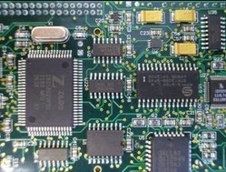
The core and key points of SMT processing
The goal of the SMT process is to produce qualified solder joints. To obtain a good solder joint, it depends on the proper pad design, the proper amount of solder paste, and the proper reflow temperature profile. These are process conditions. Using the same equipment, some manufacturers have a higher welding qualification rate, and some manufacturers have a lower welding qualification rate. The difference lies in the different processes. It is reflected in the "scientific, precise and standardized" curve setting, furnace interval, and tooling equipment during assembly. and many more. These often require companies to spend a long time to explore, accumulate and regulate. And these proven and solidified SMT process methods, technical documents, and tooling design are the "craft" and are the core of SMT. According to business division, SMT process can generally be divided into process design, process trial production and process control. The core goal is to reduce soldering, bridging, printing and displacement problems by designing the right amount of solder paste and consistent printing deposits. In each business, there is a set of process control points, among which pad design, Stencil design, solder paste printing and PCB support are the key points of process control.
With the continuous shrinking of pad size and chip processing component space, in the printing process, the area ratio of the stencil opening and the space between the stencil and the PCB are becoming more and more important.

The former is related to the solder paste transfer rate, and the latter is related to the consistency of the solder paste printing volume and the printing yield to obtain a solder paste transfer rate of more than 75%. According to experience, the area ratio between the template opening and the side wall is generally greater than or equal to 0.66: In order to obtain a stable amount of solder paste that meets the design expectations, the smaller the gap between the template and the PCB during printing, the better. It is not difficult to achieve an area ratio above 0.66, but it is very difficult to eliminate the gap between the template and the PCB. This is because the gap between the template and the PCB is related to many factors such as the design of the PCB, the warpage of the PCB, and the support for the PCB during printing. Sometimes the equipment subject to product design and use is uncontrollable, and this is precisely the fine-pitch components.
The key to assembly. Close to 100% of soldering failures, such as 0.4mm pin pitch CSP, multi-row QFN, LGA and SGA
Related to this. Therefore, in advanced professional SMT processing plants, many very effective PCB support tools have been invented to correct the curvature of the PCB bridge and ensure zero-gap printing.
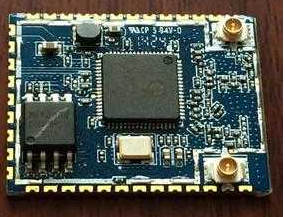
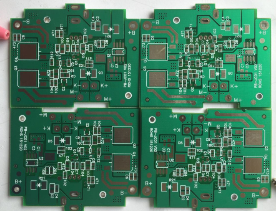
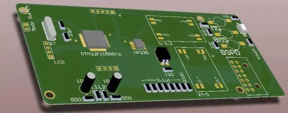
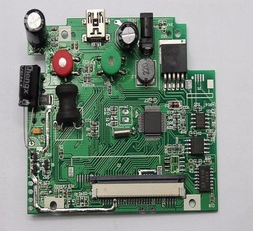
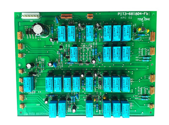
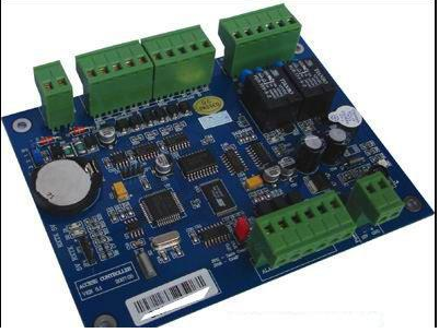
SMT processing plant
SMT chip processing capability
1. The largest board: 310mm*410mm (SMT);
2. Maximum board thickness: 3mm;
3. Minimum board thickness: 0.5mm;
4. The smallest Chip parts: 0201 package or parts above 0.6mm*0.3mm;
5. The maximum weight of mounted parts: 150 grams;
6. Maximum part height: 25mm;
7. Maximum part size: 150mm*150mm;
8. Minimum lead part spacing: 0.3mm;
9. The smallest spherical part (BGA) spacing: 0.3mm;
10. The smallest spherical part (BGA) diameter: 0.3mm;
11. Maximum component placement accuracy (100QFP): 25um@IPC;
12. Mounting capacity: 3 to 4 million points/day.