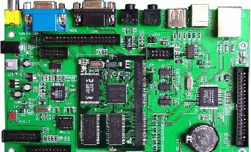
1. Causes of tin beads in SMT patch processing
1. The tin beads mainly appear on one side of the chip resistance-capacitance component, and sometimes also appear near the pins of the chip IC. Tin beads not only affect the appearance of board-level products, but more importantly, due to dense components on the printed board.
1. The tin beads mainly appear on one side of the chip resistance-capacitance component, and sometimes also appear near the pins of the chip IC. Tin beads not only affect the appearance of board-level products, but more importantly, due to the dense components on the printed board, there is a risk of short circuits during use, which affects the quality of electronic products. There are many reasons for the production of tin beads, which are often caused by one or more factors. Therefore, prevention and improvement must be done one by one to better control them.
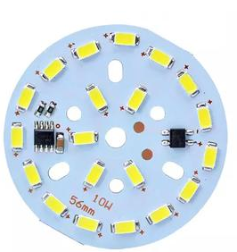
SMD tin beads
2. Tin balls refer to some large solder balls before the solder paste is soldered. The solder paste may be outside the printed pad due to various reasons such as collapse and squeeze. During soldering, these may exceed the pad. The solder paste fails to fuse with the solder paste on the pad during the soldering process and comes out independently, and is formed in the component body or near the pad.
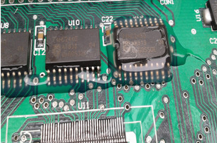
3. However, most of the solder balls occur on both sides of the chip component. Take the chip component with a square pad design as an example. As shown in the figure above, after the solder paste is printed, if the solder paste exceeds, it is easy to produce solder beads.

Melting with the solder paste on the pad part will not form solder beads.
However, when the amount of solder is large, the component placement pressure will squeeze the solder paste under the component body (insulator), and it will be melted during reflow soldering. Due to the surface energy, the melted solder paste gathers into a ball, which tends to raise the component., But this force is extremely small, and it is squeezed to both sides of the component by the gravity of the component, separated from the pad, and formed tin beads when cooled. If the component has high gravity and more solder paste is squeezed out, multiple solder balls may even be formed.
4. According to the reasons for the formation of tin beads, the main factors that affect the production of tin beads in the SMT patch production process are:
⑴The stencil opening and land pattern design.
⑵Steel mesh cleaning.
⑶The repeatability of SMT placement machine.
⑷Temperature curve of reflow oven.
⑸ Patch pressure.
⑹The amount of solder paste outside the pad.
1. There are hazards in ESD during SMT chip processing
Static electricity and electrostatic discharge are ubiquitous in our daily lives, but when used in electronic equipment, it may cause serious damage to electronic equipment. With the rapid development of electronic technology, electronic products have become
Static electricity and electrostatic discharge are ubiquitous in our daily lives, but when used in electronic equipment, it may cause serious damage to electronic equipment. With the rapid development of electronic technology, electronic products have become more and more powerful and small in size, but this is the cost of electronic components that are electrostatically sensitive. This is because high integration means that the circuit unit will become narrower and the tolerance of the electrostatic discharge capability is getting worse and worse. In addition to a large number of new materials, special devices are also static sensitive materials, so that electronic components, especially semiconductor devices, are SMT chip processing production, assembly and maintenance environment static control requirements are getting higher and higher.
But on the other hand, in the environment of SMT processing, production, use and maintenance of electronic products, various polymer materials that are prone to static electricity will be used in large quantities. This undoubtedly brings more problems and challenges to the electrostatic protection of electronic products. .
There are two types of damage and damage to electronic products caused by electrostatic discharge: sudden damage and potential damage. The so-called sudden damage refers to the severe damage of the device and loss of function. This kind of damage can usually be found in the quality inspection during the production process, so the main cost to the SMT factory is the cost of rework and repair.
Potential damage is the damaged part of the device, the function has not been lost, and cannot be found in the production process of SMT inspection, but the product will become unstable during use, good or bad, so the quality of the product is more important. Big damage. Among these two types of damage, potential failures account for more than 90%, and sudden failures account for only 10%. That is, 90% of static electricity damage is undetectable, and only the user's hand will be found in the hand, such as frequent crashes, automatic shutdown, poor call quality, large noise, good time difference, critical errors and other problems mostly related to static electricity damage .