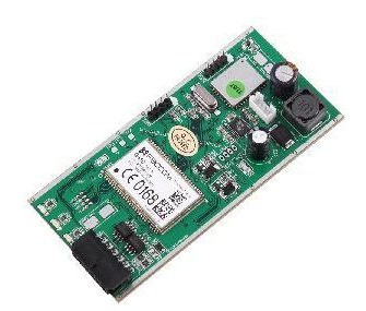
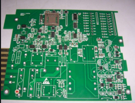
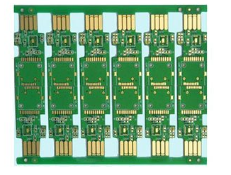
If you want to understand the high cost of PCBA processing, you need to decompose the entire process of packaging labor and materials. PCBA (PCB Assembly) means PCB assembly, so it must include circuit board light board, component welding (smt surface mount/ DIP plug-in post-welding) These two parts, the prices of light boards and components on the market are basically open and transparent in major shopping malls, and can be compared for reference.
Since the main PCB circuit boards and components are not likely to increase prices in the dark, the cost is reflected in the assembly process. The main costs of this link are in the following four aspects:
1. Auxiliary materials: solder paste, tin bar, flux, UV glue, furnace fixture
The quality of solder paste and solder bars is the most important auxiliary material in the entire processing link. Generally, the price of domestic solder paste is 180~260/bottle, and the imported solder paste may be 320~480/bottle, so on the same soldering area, The price of imported solder paste is much higher, but the difference in soldering quality is very obvious.
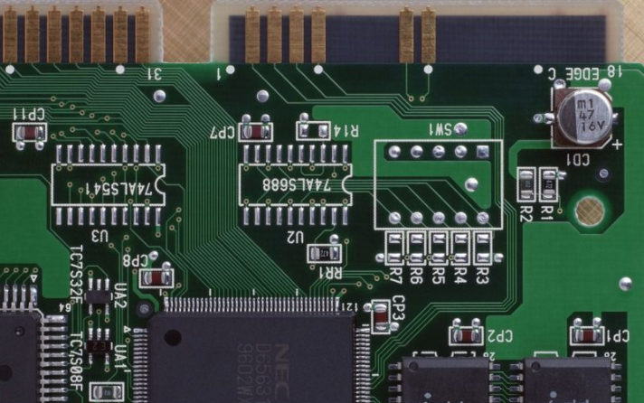
2, smt patch processing
SMD processing varies according to the number of points and packaging, and there will be a certain difference in price. Large quantity and high price are the consensus of the industry. The larger the component package size, the easier it is to mount, and the corresponding poor quality will be reduced. Therefore, there is more room for communication on the price.

3, DIP plug-in welding man hours
The plug-in material link involves special-shaped parts and material forming. This link requires a lot of manual participation. Because there is no reference to the production capacity of machinery and equipment, this link is the link that is the most difficult to control. At the same time, labor costs remain high at present, and the cost of this link is generally high.
4. Assembly test: test fixture, test equipment, test man-hour
The test fixture currently ranges from tens to hundreds of dollars depending on the difficulty of the test, and the test of communication equipment requires the assistance of optical fiber, ICT and other test equipment. The corresponding labor and equipment loss need to be taken into account, but it will not be very high. Some companies even test it for free.
How to avoid defects in smt patch processing and welding
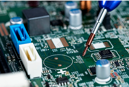
Welding is the most important link in smt patch processing. If the welding link is not done well, it will affect the entire production of the PCB board. If it is a little bit, substandard products will appear, and if it is serious, the product will be scrapped. In order to avoid the impact on the quality of smt processing due to poor welding, it is necessary to pay attention to welding.
One, welding heating bridge. The soldering thermal bridge in the SMT process is to prevent the solder from forming a bridge. If there is an error in this process, it will cause the uneven distribution of the solder. The correct soldering method is to put the soldering iron tip between the pins of the soldering pad and bring the soldering wire close to the soldering iron tip. When the solder paste melts, move the soldering wire between the soldering pad and the pins, and place the soldering iron on the soldering wire. In this way, good solder joints can be produced and the impact on processing can be reduced.
2. The pins are welded hard. In the process of processing, excessive force in the soldering of the pins can easily lead to problems such as tilting, delamination or depression of the pads of the patch. Therefore, in order to ensure the quality of the smt patch processing during the soldering process, it is not necessary to use too much force, only the soldering iron head needs to be in contact with the pad.
Third, the choice of soldering iron tip. In the soldering process, the size of the soldering iron tip is also very important. If the size is too small, the retention time of the soldering iron tip will increase, leading to the appearance of cold solder joints. Excessive size will cause the heating to be too fast and burn to the patch. Therefore, we need to choose the size suitable for the soldering iron tip according to the length and shape of the soldering iron tip, as well as the heat capacity and contact surface.
Four, temperature setting. Temperature is also a very important step in the soldering process. Too high a temperature setting will cause the pad to tilt, and excessive heating of the solder will damage the patch. Therefore, it is necessary to pay attention to the temperature setting. Setting a suitable temperature is also particularly important for processing quality. .
5. The use of flux. During the implementation of related processes, if the flux is used too much, it will cause the problem of whether the lower solder foot is stable, and if it is serious, corrosion or electron transfer may occur.
Six, transfer welding operation. Transfer soldering refers to putting the solder on the tip of the soldering iron first, and then transfer to the connection. Improper operation will cause poor wetting. Therefore, we should first place the soldering iron tip between the pad and the pin. When the soldering iron wire is close to the soldering iron tip, move the soldering wire to the opposite side while waiting for the tin to melt. Then place the tin wire between the pad and the pin. Place the soldering iron on the tin wire and move the tin wire to the opposite side when the tin melts.
Seven, modification or rework. The biggest taboo in the connection process is to retouch or rework in pursuit of perfection. And this approach is not only indispensable to repeated modification or rework in pursuit of perfect product quality, which is easy to cause the circuit/pcb circuit board metal layer to break.