1. Several standard issues that need to be paid attention to in SMT patch processing
First: Joint standards for the development of electrostatic discharge control procedures. Including the necessary design, establishment, implementation and maintenance of electrostatic discharge control procedures. According to the historical experience of certain military organizations and commercial organizations,
First: Joint standards for the development of electrostatic discharge control procedures. Including the necessary design, establishment, implementation and maintenance of electrostatic discharge control procedures. According to the historical experience of certain military organizations and commercial organizations, it provides guidance for handling and protecting electrostatic discharge sensitive periods.
Second: Welding Technology Evaluation Manual. Includes 45 articles on all aspects of soldering technology, covering general soldering, soldering materials, manual soldering, batch soldering, wave soldering, reflow soldering, vapor phase soldering and infrared soldering. Third: Semi-aqueous cleaning manual after welding. Including all aspects of semi-aqueous cleaning, including chemical, production residues, equipment, technology, process control, and environmental and safety considerations.
Fourth: Desktop reference manual for through-hole solder joint evaluation.

Detailed description of components, hole walls and welding surface coverage according to standard requirements, in addition to computer-generated 3D graphics. Covers tin filling, contact angle, tin dip, vertical filling, solder pad coverage, and numerous solder joint defects.
Fifth: Template design guidelines. Provide guidelines for the design and manufacture of solder paste and surface-mount adhesive coating templates. Also discussed template design using surface-mount technology, and introduced the combination of through-hole or flip-chip components., Including overprinting, double-printing and staged template design.
Sixth: Water into the cleaning manual after PCB soldering. Describe the cost of manufacturing residues, types and properties of aqueous cleaning agents, aqueous cleaning processes, equipment and techniques, quality control, environmental control, employee safety, and cleanliness measurement and measurement.
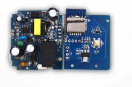
2. SMT processing surface coating process parameter design
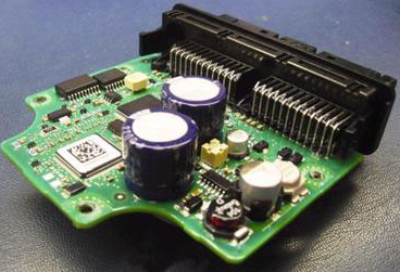
1. SMT patch printing process parameter design SMT processing stencil printing is the most basic solder paste printing method in SMT patch processing plants. Although there are many modern printing equipment, the basic printing process is the same, as shown in the figure.
1. SMT patch printing process parameter design
SMT processing stencil printing is the most basic solder paste printing method in SMT patch processing plants. Although there are many modern printing equipment, the basic printing process is the same, as shown in the figure:
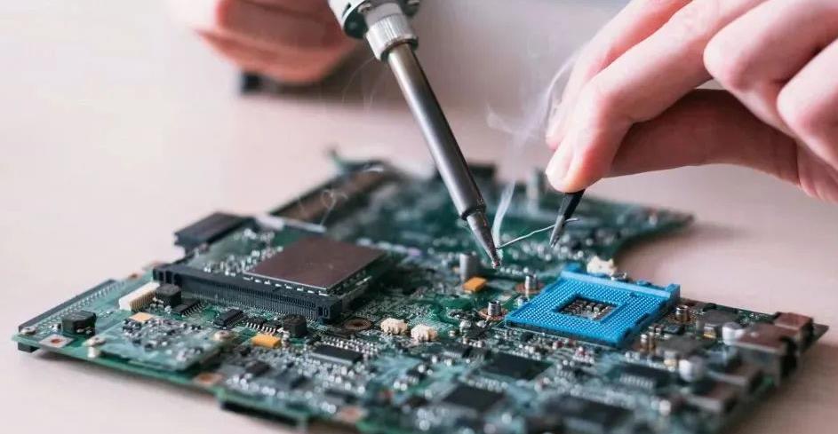
(1) Printing preparation. Before printing, the operators of the printing press should make pre-printing preparations. The preparations are mainly divided into three categories. Category 1: Fixture preparation, template, scraper, tools such as hexagon socket screwdriver, etc.; Category 2: material preparation, solder paste preparation, PCB packed in a turnover box, alcohol, wipe paper, etc.; Category 3: Document preparation, preparation Assembly technical documents, process cards, precautions, etc.
(2) Install template and scraper. Install the template, insert it into the template track and push it to the final position to clamp, unscrew the air brake switch, and fix it. For the installation of the scraper, select the appropriate scraper according to the production process of the product to be assembled. Generally, a stainless steel scraper is selected, especially for high-density assembly, the trailing scraper is used for installation.
(3) PCB positioning is aligned with graphics. The purpose of PCB positioning is to initially adjust the PCB to the position corresponding to the template image. The substrate positioning methods include hole positioning, edge positioning, and vacuum positioning.
Hole positioning: semi-automatic equipment, vision system is required when higher accuracy is required, and special positioning posts are required.
Edge positioning: automatic equipment, optical positioning is required, and the substrate thickness and flatness requirements are high.
Vacuum positioning: strong vacuum suction is the key to ensuring printing quality.
(4) Set process parameters. The main parameters are squeegee pressure and squeegee speed. Squeegee angle, squeegee selection, separation speed, printing gap, printing stroke, cleaning mode and frequency, etc.
(5) Add solder paste and print. Use a small spatula to apply the solder paste evenly along the width of the squeegee behind the missing pattern of the template. Solder paste cannot be applied to the leaking hole of the template.
(6) Analysis of stencil printing results. The solder paste printing result requirements are as follows. The amount of printed solder paste is uniform and consistent; the solder paste pattern is clear, and there is no adhesion between adjacent patterns; the solder paste pattern and the PCB pad pattern should not be misaligned.
(7) Analysis of solder paste printing defects.