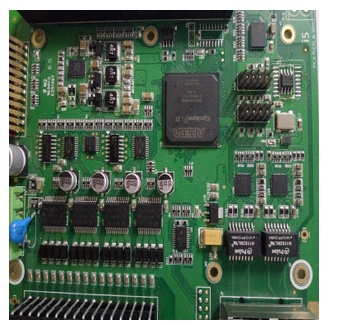
Various consumer electronic products such as cellular phones, personal digital assistants (PDAs), and digital cameras have gradually become smaller, more responsive, and more intelligent. Therefore, electronic packaging and assembly processes must keep up with this rapid development. With the continuous improvement of material performance, equipment and process level, more and more electronic manufacturing service companies (EMS) are no longer satisfied with the conventional smt placement process, and constantly try to use new assembly processes, including Flip chip (FC).
In order to meet the market's demand for providing "all-round solutions", EMS companies and semiconductor packaging companies have a tendency to gradually move closer to each other in terms of technology and business, but this poses no small challenges to both parties. When electronic products transition from board assembly to component assembly (such as FCBGA or SIP), many new problems will arise, including stress generated during interconnection, material incompatibility, and changes in processing technology.

Regardless of whether you plan to use FC technology in a new product or you are considering the best time to use FC technology, it is necessary to understand FC technology and fully understand the various problems that may arise from using it.
1. Introduction to FC technology
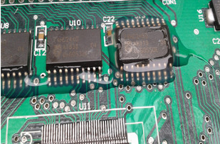
FC refers to a method of directly mounting and interconnecting the chip and the substrate. Compared with the other two widely used chip-level interconnection methods, WB and TAB, the FC chip faces down, and the pads on the chip are directly interconnected with the pads on the substrate. At the same time, FC is not only a high-density chip interconnection technology, it is also an ideal chip bonding technology, and because of this, FC has been widely used in PGA, BGA and CSP. Because FC's interconnection line is very short, and the I/O terminals are distributed on the entire chip surface, and FC is also suitable for mass production using smt technology, so FC will be the final development of packaging and high-density assembly technology direction.
Strictly speaking, FC is not a new technology. As early as 1964, in order to overcome the shortcomings of poor manual bonding reliability and low productivity, IBM used the solid-state logic technology (SLT) hybrid component in its 360 system for the first time. The technology. But from the 1960s to the 1980s, no major breakthroughs have been made. Until the past ten years, with the continuous development of materials, equipment and processing technology, and with the increasing trend of miniaturization, high speed, and multi-function of electronic products, FC has once again received widespread attention.
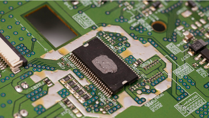
FC has a history of more than 40 years since it was first developed by IBM's Bell Labs, and there are many types. If the substrate can choose ceramic or PCR bumps, it can be divided into two categories: solder bumps and non-solder bumps. Non-solder bumps include gold bumps and polymer bumps. The preparation of solder bumps can use electroplating, Evaporation/sputtering method, jet bumping method, etc. Different types of FC have their own advantages and disadvantages. Among them, the solder bump flip chip or controllable collapse chip (C4) technology can be directly mounted on the PCB and flip-chip soldered by smt, which can realize the FC manufacturing process. The effective combination with smt has become the most popular and most potential FC technology in the world, which is exactly what this article is mainly discussing.
C4 technology first used ceramics similar to the CTE of silicon as the substrate material. However, due to the high price of ceramics and the high dielectric constant, it is easy to cause signal delay. At this time, organic PCB substrates begin to enter people's field of vision. However, the CTE difference between PCB and silicon is too large, and it is easy to cause fatigue damage to the solder joints due to excessive internal stress during temperature cycling. Therefore, until the 1980s, that is, before the invention of the underfill technology, FC has not been put into practical use.
The fatigue life of the solder joints is increased by 10 to 100 times after using the lower filler. However, in the smt patch proofing or processing production, on the one hand, the filling process is very time-consuming, and on the other hand, it also brings certain difficulties to the repair. This has become two important directions of filling technology under current research. In addition to the above-mentioned underfilling technology, the preparation of the "rewiring layer" on the chip and the compatibility with existing smt equipment are the two keys that affect the promotion and application of FC.