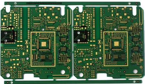
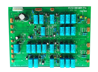
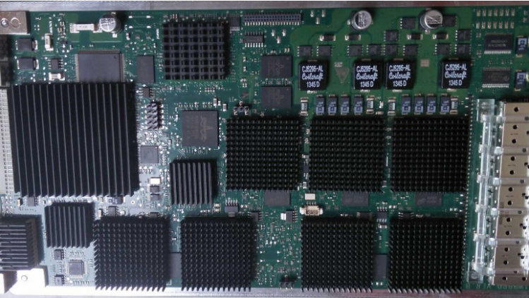
Causes and solutions for the short-circuit phenomenon in SMT chip processing. SMT processing short-circuit phenomenon occurs mostly between the pins of fine-pitch ICs, so it is also called "bridging". Of course, there are also short circuits between CHIP parts, which is very rare. Now let's talk about the reason and solution of the bridging problem between fine-pitch IC pins. The bridging phenomenon mostly occurs between IC pins with a pitch of 0.5mm and below. Because of the small pitch, improper template design or slight omissions in printing can easily occur. A. The template is based on the requirements of IPC-7525 Steel Mesh Design Guide. In order to ensure that the solder paste can be smoothly released from the openings of the stencil to the PCB pads, the opening of the stencil mainly depends on three factors: 1. )Area ratio/width-thickness ratio>0.66 2.)The mesh wall is smooth.

Suppliers are required to perform electro-polishing during the production process. 3.) With the printing surface as the upper side, the lower opening of the mesh should be 0.01mm or 0.02mm wider than the upper opening, that is, the opening is in an inverted cone shape, which is convenient for the effective release of solder paste and reduces the frequency of cleaning the screen. Specifically, for ICs with a pitch of 0.5mm and below, due to their small PITCH, bridging is easy to occur, the length of the stencil opening method is unchanged, and the opening width is 0.5 to 0.75 pad width. The thickness is 0.12~0.15mm. It is best to use laser cutting and polishing to ensure that the shape of the opening is inverted trapezoid and the inner wall is smooth, so that the tinting and forming are good at the time of printing. B. Solder Paste The correct choice of solder paste is also very important for solving bridging problems. When using solder paste for ICs with a pitch of 0.5mm and below, the particle size should be 20~45um, and the viscosity should be around 800~1200pa.s. The activity of the solder paste can be determined according to the cleanliness of the PCB surface, generally RMA grade is used. C. Printing Printing is also a very important part.
(1) Type of squeegee: There are two types of squeegee: plastic squeegee and steel squeegee. For ICs with PITCH≤0.5mm, steel squeegee should be used for printing to facilitate the formation of solder paste after printing. (2) Adjustment of the squeegee: The operating angle of the squeegee is printed in the direction of 45°, which can significantly improve the imbalance of the opening direction of the different stencils of the solder paste, and it can also reduce the damage to the fine-spaced stencil opening; the pressure of the squeegee is generally 30N /mm². (3) Printing speed: The solder paste will roll forward on the template under the push of the squeegee. Fast printing speed is conducive to the rebound of the template, but at the same time it will prevent the solder paste from being printed. If the speed is too slow, the solder paste will not roll on the template, causing poor resolution of the solder paste printed on the pad. The printing speed range of the pitch is 10~20mm/s (4) Printing method: At present, the most common printing method is divided into "contact printing" and "non-contact printing". The printing method where there is a gap between the template and the PCB is "non-contact printing". The general gap value is 0.5~1.0mm, and its advantage is that it is suitable for solder paste with different viscosity. The solder paste is pushed into the template opening by the squeegee to contact the PCB pad. After the squeegee is slowly removed, the template will be automatically separated from the PCB, which can reduce the problem of template contamination due to vacuum leakage. The printing method with no gap between the template and the PCB is called "contact printing". It requires the stability of the overall structure and is suitable for printing high-precision solder paste. The template maintains a very flat contact with the PCB, and only separates from the PCB after printing. Therefore, the printing accuracy achieved by this method is high, and it is especially suitable for fine pitches., Ultra-fine pitch solder paste printing. D. Mounting height. For ICs with PITCH≤0.5mm, 0 distance or 0~-0.1mm mounting height should be used during mounting to avoid the solder paste molding collapse due to too low mounting height. A short circuit occurs during reflow. E. Reflow 1. The heating speed is too fast. 2. The heating temperature is too high. 3. The solder paste is heated faster than the circuit board. 4. The flux wetting speed is too fast.