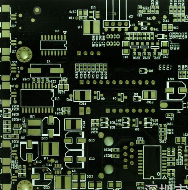
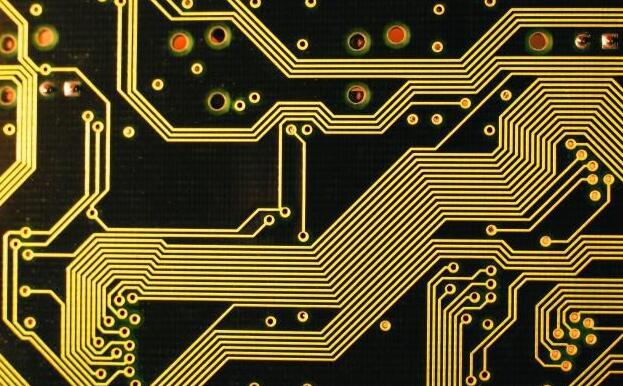
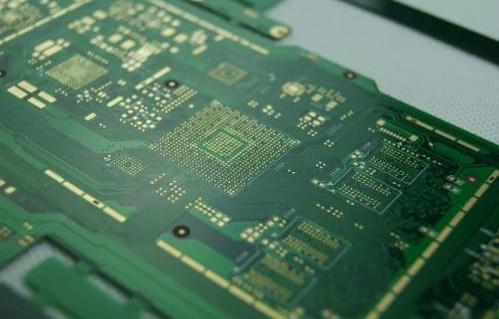
The most important design in PCB processing is the board drawing design. We need to pay attention to several issues in the board drawing design:
First: create packages that are not in the package library. Before designing the PCB diagram, if a component in the schematic diagram cannot find the package model in the package library, you need to use the component package model editor to create a new one. Make sure that the package model of the component used is in the package library ( It can be multiple library files) in order to ensure the smooth progress of PCB design.

Second: Set the design parameters of the PCB board drawing. According to the needs of the circuit system design, set the number of layers, size, color, etc. of the PCB board.
Third: Load the netlist. Load the netlist generated by the schematic, and automatically load the component package model into the PCB design window.
Fourth: layout. The method of combining automatic layout and manual layout can be used to place the component packaging model in an appropriate position within the PCB planning range, that is, to make the component layout neat, beautiful, and conducive to wiring.
Fifth: Wiring. Set the wiring design rules and start automatic wiring. If the wiring is not completely successful, manual adjustments can be made.
Sixth: Design rule check. Carry out design planning check on the designed PCB board (check whether the components overlap, whether the network is short-circuited, etc.), if there are errors, modify them according to the error report.
Seventh: PCB board simulation analysis. Carry on simulation analysis to the signal processing of PCB board, mainly analyze the influence of layout and wiring on various parameters, so as to improve and modify.
Eighth: Save the output. The designed PCB diagram can be saved, printed in layers, and output PCB design files.
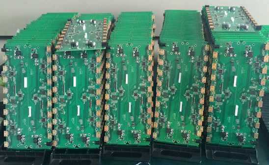
Advantages of SMT chip processing technology
With the continuous progress and development of the electronics industry, SMT surface assembly technology has become more mature, and equipment functions are constantly improving. SMT patch processing technology has gradually replaced traditional cartridge technology and has become the most popular process technology in the electronics assembly industry. "Smaller, lighter, denser, and better" are the biggest advantages of SMT chip processing technology, and it is also the current requirement for high integration and miniaturization of electronic products.
SMT chip processing process: first apply solder paste on the surface of the printed circuit board pad, then accurately place the metalized terminals or pins of the component on the solder paste of the pad, and then connect the printed circuit board to the component Put them into a reflow oven and heat the whole to the melting of the solder paste. After cooling and solidification of the solder paste, the mechanical and electrical connections between the components and the printed circuit are realized. As a professional SMT chip processing factory, Lingxinte can provide users with various SMT services such as SMT processing fast proofing, difficult SMT chip processing, and special SMT chip processing. Let's talk to the technicians of Lingxinte to understand the advantages of SMT chip processing technology:
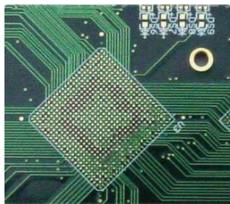
1. Electronic products are small in size and high in assembly density
The volume of SMT chip components is only about 1/10 of the traditional plug-in components, and the weight is only 10% of the traditional plug-in components. Usually, the use of SMT technology can reduce the volume of electronic products by 40%~60% and the quality by 60%~80 %, the occupied area and weight are greatly reduced. The SMT patch processing assembly component grid has developed from 1.27MM to the current 0.63MM grid, and individual grids have reached 0.5MM. The through-hole mounting technology is used to install the components, which can make the assembly density higher.
2. High reliability, strong anti-vibration ability
SMT chip processing uses chip components with high reliability. The components are small and light, so it has strong anti-vibration ability. It adopts automated production and has high mounting reliability. Generally, the rate of bad solder joints is less than 10 parts per million. The wave soldering technology of through-hole plug-in components is one order of magnitude lower, which can ensure a low defect rate of solder joints of electronic products or components. At present, almost 90% of electronic products adopt SMT technology.
Three, high-frequency PCB characteristics are good, reliable performance
Because the chip components are firmly mounted, the devices are usually leadless or short leads, which reduces the influence of parasitic inductance and parasitic capacitance, improves the high-frequency characteristics of the circuit, and reduces electromagnetic and radio frequency interference. The maximum frequency of the circuit designed with SMC and SMD is 3GHz, while the chip component is only 500MHz, which can shorten the transmission delay time. It can be used in circuits with a clock frequency above 16MHz. If the MCM technology is used, the high-end clock frequency of the computer workstation can reach 100MHz, and the additional power consumption caused by parasitic reactance can be reduced by 2-3 times.
4. Improve productivity and realize automated production
At present, if the perforated PCB printed board is to be fully automated, the area of the original printed board needs to be enlarged by 40%, so that the insertion head of the automatic plug-in can insert the components, otherwise there is not enough space and the parts will be damaged. The automatic placement machine (SM421/SM411) uses a vacuum nozzle to pick and place the components. The vacuum nozzle is smaller than the shape of the component, which increases the mounting density. In fact, small components and fine-pitch QFP devices are produced using PCBA automatic placement machines to achieve full-line automated production.