In order to better apply "Internet +" to the processing and manufacturing of SMT electronic products, focus on the integration and gathering of offline resources, the construction and promotion of online platforms, and actively explore new e-commerce marketing models.
Gathering senior management and technical teams in the industry, relying on the one-stop Internet service platform realized by "f2cpcb cloud manufacturing" electronic products, integrating product design companies, supply chains, manufacturing plants and other resources to provide customers with electronic product design, material procurement, One-stop manufacturing service. Provide enterprises with cost-effective services, produce high-quality products for enterprises, and help enterprises improve their core competitiveness.
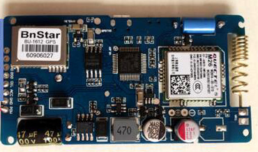
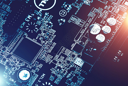
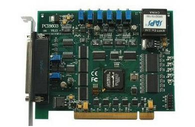
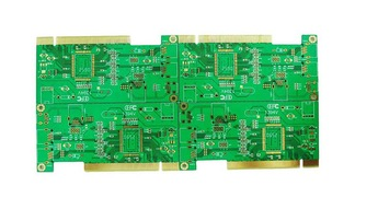
SMT processing chip technology greatly promotes the efficiency of electronic assembly. The surface mount process includes: printing solder paste on the PCB, mounting components, reflow soldering, etc. The key equipment of the SMT process is the placement machine. The placement accuracy, placement speed, and the application range of the placement machine determine the technical capabilities of the placement machine, and the placement machine also determines the efficiency of the SMT production line. The manufacturing of electronic products can be divided into three levels.

The top layer is the manufacturing of complete products that directly face end users, such as the manufacturing of computers, communication equipment, and various audio and video products. The middle level is a wide variety of electronic basic products that form electronic terminal products, including semiconductor integrated circuits, electric vacuum and optoelectronic display devices, electronic components, and electromechanical components. Electronic products are assembled and integrated from basic electronic products. The lowest level is the special equipment, electronic measuring instruments and electronic special materials that support the assembly of electronic terminal products and the production of electronic basic products. They are the foundation and support of the entire electronic information industry.
The composition and manufacturing process of electronic products can be summarized as the following technologies.
1. Microfabrication technology.
Micro and nano processing, micro processing, and some precision processing techniques used in electronic manufacturing are collectively referred to as micro processing. Micro-nano processing in micro-processing technology is basically a method of planar integration. The basic idea of planar integration is to build micro-nano structures on planar substrate materials by layer-by-layer stacking. In addition, processing methods such as cutting, welding, 3D printing, etching, and sputtering using photon beams, electron beams and ion beams also belong to microfabrication.
2. Interconnection and encapsulation technology.
The interconnection between the chip and the lead-out circuit on the substrate, such as flip-chip bonding, wire bonding, through silicon via (TSV) and other technologies, and the encapsulation technology after the chip and the substrate are interconnected. These technologies are commonly referred to as Chip packaging technology. Passive component manufacturing technology. Including the manufacturing technology of passive components such as capacitors, resistors, inductors, transformers, filters, and antennas.
3. Optoelectronic packaging technology.
Optoelectronic packaging is the system integration of optoelectronic devices, electronic components and functional application materials. In the optical communication system, optoelectronic packaging can be divided into chip IC-level packaging, device packaging, and mold MEMS manufacturing technology. A micro system that integrates sensors, actuators, and processing control circuits on a single silicon chip by using microfabrication technology.
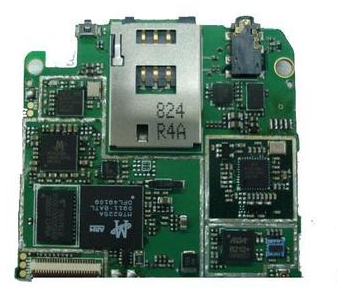
4. SMT electronic assembly technology.
Electronic assembly technology is commonly referred to as board-level packaging technology. Electronic assembly technology is mainly based on surface assembly and through-hole insertion technology. Electronic materials technology. Electronic materials refer to materials used in electronic technology and microelectronics technology, including dielectric materials, semiconductor materials, piezoelectric and ferroelectric materials, conductive metals and their alloy materials, magnetic materials, optoelectronic materials, electromagnetic wave shielding materials and other related materials Material. The preparation and application technology of electronic materials is the basis of electronic manufacturing technology.