Shenzhen PCB processing process flow pad
Paying attention to the trend of environmental protection informatization and the development of various environmental protection technologies, PCB factories can start with big data to monitor the company's pollution discharge and governance results, and find and solve environmental pollution problems in a timely manner. Keep up with the production concept of the new era, continuously improve resource utilization, and realize green production. Strive to make the PCB factory industry realize an efficient, economical and environmentally friendly production model, and actively respond to the country's environmental protection policy.
When ordering a stencil for a printing process, there is a clear experience curve. When the familiarity with its technology helps to produce the desired result, the template Shenzhen PCBA processing technology is a constant in the variable assembly operation.
Shenzhen PCBA processing process "good templates get good printing results, and then automation helps make the results repeatable."
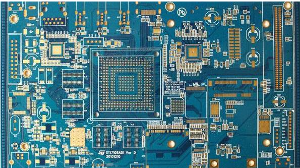
Backplane Production Technology

The backplane has always been a specialized product in the PCB manufacturing industry. Its design parameters are very different from most other circuit boards. It needs to meet some stringent requirements in production. The noise tolerance and signal integrity also require the backplane design to comply with the special land (land) and the basic surface mount assembly. The constituent unit is used to form the land pattern of the circuit board, that is, various land combinations designed for special component types. There is nothing more frustrating than a poorly designed pad structure. Shenzhen PCBA processing process when a pad structure is not designed correctly, it is difficult, sometimes even impossible to reach the expected solder joint.
Shenzhen PCBA processing process pad in English has
One, the line part:
1, disconnection,
A, there is a break or discontinuity on the line,
B, The length of the broken wire on the line exceeds 10mm and cannot be repaired.
C, The disconnection is near the PAD or the edge of the hole, (the disconnection is at the PAD or the edge is less than or equal to 2mm and can be repaired. The disconnection is greater than 2mm from the PAD or the edge of the hole, and it cannot be repaired.)
D, Adjacent lines are disconnected side by side and cannot be repaired
An instrument with excellent performance, in addition to selecting high-quality components and reasonable circuits, the correct structural design of the component layout of the printed circuit board and the electrical connection direction is a key issue that determines whether the instrument can work reliably. For the same component And the parameters of the circuit, the Shenzhen PCB processing process will be different due to the component layout design and the electrical connection direction. Our factory is located in China. For decades, Shenzhen has been known as the world's electronics R&D and manufacturing center. Our factory and website are approved by the Chinese government, so you can skip the middlemen and buy products on our website with confidence. Because we are a direct factory, this is the reason why 100% of our old customers continue to purchase on iPCB.
No minimum requirements
You can order as little as 1 PCB from us. We will not force you to buy things you really don't need to save money.