There are many ways to solve the EMI problem. Modern EMI suppression methods include: using EMI suppression coating, selecting appropriate EMI suppression spare parts, EMI simulation design, etc. Starting from the basic PCB cloth board, this paper discusses the role of PCB stacking in EMI radiation control and design techniques.
PCB power bus
Reasonable capacitance placement near the pin of the IC can make the IC output voltage jump faster. However, this is not the end of the problem. Due to the limited frequency response of the capacitor, it is not possible for the capacitor to generate the harmonic power needed to drive the IC output cleanly in the full frequency band. In addition, the transient voltage formed on the power confluence creates a voltage drop at both ends of the inductor in the decoupling path, which is the main common mode EMI interference source. How should we solve these problems?
There are many ways to solve the EMI problem. Modern EMI suppression methods include: using EMI suppression coating, selecting appropriate EMI suppression spare parts, EMI simulation design, etc. Starting from the basic PCB cloth board, this paper discusses the role of PCB stacking in EMI radiation control and design techniques.
power bus
Reasonable capacitance placement near the pin of the IC can make the IC output voltage jump faster. However, this is not the end of the problem. Due to the limited frequency response of the capacitor, it is not possible for the capacitor to generate the harmonic power needed to drive the IC output cleanly in the full frequency band. In addition, the transient voltage formed on the power confluence creates a voltage drop at both ends of the inductor in the decoupling path, which is the main common mode EMI interference source. How should we solve these problems?
For IC on our printed circuit board, the power layer around IC can be viewed as a good high frequency capacitor, which can collect the part of energy leaked from discrete capacitors that provide high frequency energy for clean output. In addition, the inductance of a good power layer is smaller, so that the transient signal synthesized by the inductance is smaller, which reduces the common mode EMI.
Of course, the connection between the PCB power layer and the IC power pin must be as short as possible, because the digital signal rises faster and faster, preferably directly to the pad where the IC power pin is located, which is discussed separately.
In order to control common mode EMI, the power layer must be a well designed pair of power layers to help decouple and have sufficiently low inductance. One might ask, how good is that? The answer to the question depends on the layers of the power supply, the material between layers, and the operating frequency (that is, a function of the rise time of the IC). Usually, the gap between power layers is 6mil, and the sandwich is FR4 material. The equivalent capacitance of the power layer per square inch is about 75pF. Obviously, the smaller the layer spacing, the larger the capacitance.
There are not many devices with rise time between 100 and 300 ps, but according to the current development speed of IC, devices with rise time between 100 and 300 PS will occupy a high proportion. For circuits with 100 to 300 PS rise time, 3mil layer spacing is no longer applicable for most applications. At that time, it was necessary to use a layer technique with a layer spacing less than 1 mil and to replace FR4 dielectric materials with materials with high dielectric constants. Now, ceramic and ceramic plastics can meet the design requirements of 100 to 300 PS rise time circuit.
Although new materials and new methods may be introduced in the future, common-mode EMI can be very low for today's common 1 to 3 ns rise-time circuits, 3 to 6 mil layer spacing, and FR4 dielectric materials, which are usually sufficient to handle high-end harmonics and keep transient signals low enough. The PCB stacking design example given in this paper assumes a layer spacing of 3 to 6 mil.
PCB Electromagnetic Shielding
From the signal routing point of view, a good layering strategy should be to place all the signal routing on one or several layers, which are next to the power or ground layer. For power supply, a good layering strategy should be that the power layer is adjacent to the ground layer and the distance between the power layer and the ground layer is as small as possible. This is what we call the "layering" strategy.

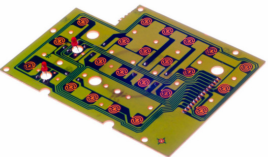
PCB stacking
What stacking strategies can help shield and suppress EMI? The following layered stacking schemes assume that the power current flows on a single layer and that the single voltage or multiple voltage are distributed on different parts of the same layer. The case of multiple power layers will be discussed later.
4 layers PCB board
There are several potential problems with the 4-layer design. Firstly, the gap between the power layer and the grounding layer is too large even if the signal layer is outside and the power and grounding layer are inside.
If the cost requirement is first, consider the following two alternatives to conventional 4-layer plates. Both can improve the EMI suppression performance, but only when the density of the elements on the board is low enough and there is enough area around the elements to place the required copper clad power supply.
The first is the preferred scheme, in which the outer layer of the PCB is a stratum and the middle layer is a signal/power layer. The power supply on the signal layer is wired by a wide line, which makes the path impedance of the power current low and the impedance of the signal microstrip path low. From the perspective of EMI control, this is the best four-layer PCB structure available. The second scheme uses both the outer layer and the middle layer to walk the signal. Compared with the traditional 4-layer plate, the improvement is smaller, and the inter-layer impedance is as poor as the traditional 4-layer plate.
If line impedance is to be controlled, the above stacking schemes carefully place the line below the power supply and ground copper islands. In addition, the copper islands on the power supply or stratum should be interconnected as closely as possible to ensure DC and low frequency connectivity.
6layers PCB board
If the component density on the 4-layer panel is high, it is better to use the 6-layer panel. However, some of the stacking schemes in the 6-layer panel design do not shield the electromagnetic field well enough and have little effect on the reduction of the transient signal of the power bus. Two examples are discussed below.
The first example places the power supply and the ground on layers 2 and 5 respectively, which is very detrimental to the control of common mode EMI radiation due to the high copper-coated impedance of the power supply. However, from the point of view of signal impedance control, this method is very correct.
In the second example, the power supply and ground are placed on layers 3 and 4 respectively. This design solves the problem of copper-clad impedance of power supply. Due to the poor electromagnetic shielding performance of layers 1 and 6, the differential mode EMI is increased. If the number of signal lines on the two outer layers is minimum, the line length is very short (less than 1/20 of the maximum harmonic wavelength of the signal). This design solves the differential mode EMI problem. Copper paving on the outer non-component and non-wired areas and grounding on the copper-clad area (every twentieth wavelength interval) suppresses the differential mode EMI particularly well. As mentioned earlier, the copper paving area should be associated with the internal grounding layer multipoints.
Universal high performance 6-layer design generally lays layers 1 and 6 into strata and layers 3 and 4 are powered and grounded. EMI suppression is excellent because there are two layers of centered dual-microstrip signal lines between the power layer and the adjacent strata. The drawback of this design is that there are only two layers in the line layer. As previously described, if the outer layer is short and copper is paved in the wireless area, the traditional 6 is used. Layers can also achieve the same stacking.
Another 6-layer layout is signal, ground, signal, power, ground, signal, which enables the environment required for advanced signal integrity design. The signal layer is adjacent to the ground layer, and the power layer and the interface layer are paired. Obviously, the drawback is that the stacking of layers is unbalanced.
This usually causes problems in processing and manufacturing. The solution is to fill all blank areas in the third layer with copper, which can be loosely considered as a structurally balanced circuit board if the copper density of the third layer is close to the power or ground layer. The copper filling area must be connected either to the power supply or to the ground. The distance between the connecting holes is still 1/20 of the wavelength and is not always connected anywhere. Connect, but ideally connect.
10layersPCB board
Because the insulation isolation layer between the multilayers is very thin, the impedance between the 10 or 12 layers of the circuit board and the layers is very low, and as long as the layers and stacks are not faulty, excellent signal integrity is fully expected. It is more difficult to process 12 layers at a thickness of 62mil and fewer manufacturers are able to process 12 layers.
Because there is always an insulating layer between the signal layer and the loop layer, it is not optimal to assign six layers in the middle of the 10-layer design to walk the signal line. In addition, it is important to have the signal layer adjacent to the loop layer, that is, the layout of the board is signal, ground, signal, signal, ground, signal.
This design provides a good path for the signal current and its loop current. The appropriate wiring strategy is that the first layer follows the X direction, the third layer follows the Y direction, the fourth layer follows the X direction, and so on. Visually, layers 1 and 3 are a pair of layers, layers 4 and 7 are a pair of layers, layers 8 and 10 are the last pair of layers. When you need to change the direction of the line, the signal line on the first layer should change direction after the third layer by means of "pass through the hole". In fact, this may not always be possible, but it should be adhered to as much as possible as possible as a design concept.
Similarly, when the direction of the signal changes, the signal should be routed from Layer 8 and Layer 10 or Layer 4 to Layer 7 by means of holes. This wiring ensures that the coupling between the forward path of the signal and the loop is tightest. For example, if the signal is on Layer 1 and the loop is on Layer 2 and only on Layer 2, then the signal on Layer 1 even by means of "holes" "Turning to Layer 3, the circuit is still on Layer 2, which maintains the characteristics of low inductance, large capacitance and good electromagnetic shielding performance.
What if this is not the case? For example, the signal line on the first layer passes through the hole to the 10th layer, then the loop signal has to look for the ground plane from the 9th layer, and the loop current needs to find the nearest ground through the hole (such as the ground pin for components such as resistance or capacitance) If such a hole happens to exist nearby, it's really lucky. If no such near hole is available, the inductance will increase, the capacitance will decrease and the EMI will increase.
When the signal line must leave the present pair of layers to other layers via the holes, the grounding holes should be placed close to the holes so that the loop signal can be smoothly returned to the appropriate layer of connection. For layers 4 and 7, the signal loop will be from the power or grounding layer (i.e. Layer 5 or Layer 6) Back because the capacitive coupling between the power layer and the interface layer is good, the signal is easy to transmit.
Design of Multiple Power Layer
If two power layers of the same voltage source need to output large currents, the circuit board should be laid out in two sets of power layers and connection layers. In this case, an insulating layer is placed between each pair of power layers and connection layers. This results in two pairs of power confluences with equal impedances as we expect. If the stacking of power layers causes unequal impedances, the shunting will be uneven. The transient voltage is much larger and the EMI increases dramatically.
If there are multiple power supply voltages with different values on the circuit board, multiple power layers are required accordingly, keep in mind that each pair of power layers and connection layers is created for different power sources. In both cases, when determining the position of the paired power layers and connection layers on the circuit board, keep in mind the manufacturer's requirements for a balanced structure.
summary
Since most engineers design printed circuit boards that are 62mil thick and without blind holes or buried holes, the discussion on the layering and stacking of PCB is limited to this. The layering schemes recommended in this paper may not be ideal for circuit boards with large thickness differences. In addition, the layering methods presented in this paper are not applicable due to the different processing processes of printed circuit boards with blind holes or buried holes.