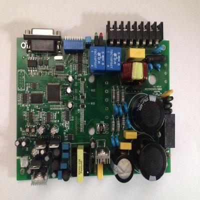
1. Component arrangement rules for high frequency PCB board
1). Under normal conditions, all components should be placed on the same side of the printed circuit. Only when the top components are too dense, can some devices with limited height and low heat output, such as patch resistance, patch capacitance, patch IC, etc. be placed on the bottom.
2). On the premise of guaranteeing the electrical performance, the components should be placed on the raster and arranged parallel or vertically with each other in order to be neat and beautiful. In general, overlapping elements are not allowed. Compact element arrangement, keep input and output components as far away as possible.
3). There may be a high potential difference between components or wires, so their distances should be increased to avoid accidental short-circuit caused by discharge and breakdown.
4). Components with high voltage should be placed as far as possible in areas that are not easily accessible to the hands during debugging.
5). Components located at the edge of the plate, at least 2 plate thicknesses away from the edge of the plate
6). The elements should be evenly distributed and compact throughout the board.
2. High frequency PCB board layout according to signal direction principle
1). Usually each functional circuit unit position is arranged one by one according to the signal flow, centering on the core components of each functional circuit and laying out around it.
2) The layout of the elements should facilitate the flow of signals so that the signals remain in the same direction as possible. In most cases, the flow direction of the signal is arranged from left to right or from top to bottom. Components directly connected to input and output should be placed close to input and output connectors or connectors.
3. Prevention of electromagnetic interference from high frequency PCB board
1). Components with strong radiation electromagnetic fields and sensitive to electromagnetic induction should be placed in a direction that crosses the adjacent printed guidance lines by increasing their distance from each other or shielding them.
2) Avoid high and low voltage devices intermingled with each other and devices with strong and weak signals interlaced as much as possible.
3). For components that will generate magnetic fields, such as transformers, speakers, inductances, etc., attention should be paid to reducing the cutting of magnetic lines to printed guidance lines when laying out. The magnetic fields of adjacent components should be perpendicular to each other to reduce the coupling between them.
4). Shield the interference source and the shield should be well grounded.
5). Circuits operating at high frequencies should consider the influence of distribution parameters between components.
4. Suppression of thermal interference by high frequency PCB board
1). For heating elements, preference should be given to locations that are heat-dissipating and, if necessary, individual radiators or small fans can be set up to reduce temperature and influence on adjacent components.
2). Some high-power integrated blocks, large or medium-power tubes, resistors and other components should be placed in a place where heat is easily dispersed and separated from other components.
3). Thermal sensitive elements should be kept close to the measured element and away from the high temperature area to avoid the influence of other heat equivalent elements and cause misoperation.
4). When double-sided elements are placed, the heating elements are generally not placed on the bottom layer.
5. Layout of adjustable elements for high frequency PCB board
For the layout of adjustable elements such as potentiometer, variable capacitor, adjustable inductance coil or micro-switch, the whole machine structure should be taken into account. If the outside of the machine is adjusted, the position of the adjustment knob should correspond to the position of the adjustment knob on the chassis panel. If in-machine adjustment, place the high frequency PCB board in the adjustment place.