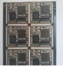
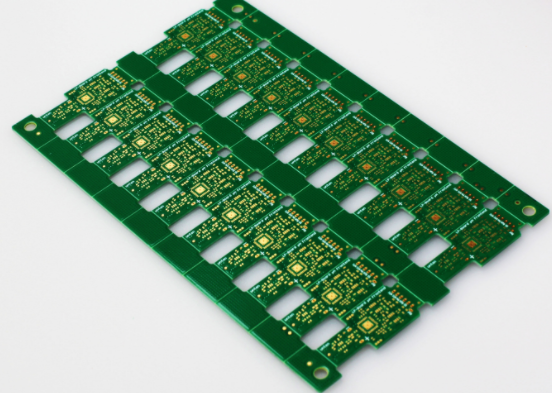
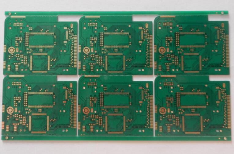
Prevent multi-layer circuit boards from warping during the production process
Circuit board manufacturer editor: 1. Prevent or increase the warpage of the substrate due to improper inventory method
(1) Since the copper clad laminate is in the storage process, because moisture absorption will increase the warpage, the moisture absorption area of the single-sided copper clad laminate is large. If the inventory environment humidity is high, the single-sided copper clad laminate will significantly increase the warpage. The moisture of double-sided copper clad laminate can only penetrate from the end surface of the product, the moisture absorption area is small, and the warpage changes slowly. Therefore, for the copper clad laminates without moisture-proof packaging, attention should be paid to the warehouse conditions, minimize the humidity in the warehouse and avoid bare copper clad laminates to avoid increased warpage of the copper clad laminates in storage.
(2) Improper placement of copper clad laminates will increase warpage. Such as vertical placement or heavy objects on the copper clad laminate, improper placement, etc. will increase the warpage and deformation of the copper clad laminate.
2. Eliminate substrate stress and reduce PCB board warpage during processing
Because in the process of multi-layer circuit board processing, the substrate has to be exposed to heat and many kinds of chemical substances many times. For example, after the substrate is etched, it needs to be washed, dried and heated. Electroplating is hot during pattern plating. After printing green oil and marking characters, it must be heated or dried with UV light. Thermal shock to the substrate when hot air is sprayed. It's also very big and so on. These processes may cause the PCB circuit board (Shenzhen Circuit Board Factory) to warp.
3. Avoid warping caused by improper circuit design or improper processing technology of printed multilayer circuit boards.
For example, the conductive circuit pattern of the multilayer circuit board is not balanced or the circuit on both sides of the PCB board is obviously asymmetrical, and there is a large area of copper on one side, which forms a large stress, which causes the multilayer circuit board to warp, and the processing temperature in the PCB circuit board manufacturing process High or large thermal shock will cause the multi-layer circuit board to warp. For the impact caused by improper storage method of the laminated board, the multi-layer circuit board factory is better to solve it, and it is enough to improve the storage environment and eliminate the vertical placement and avoid heavy pressure. For PCB boards with a large area of copper in the circuit pattern, it is best to mesh the copper foil to reduce stress.

4. When wave soldering or dip soldering, the solder temperature is too high and the operation time is too long, which will increase the warpage of the substrate. For the improvement of the wave soldering process, the electronic assembly factory needs to cooperate.
Since stress is the main cause of substrate warpage, if the copper clad laminate is baked (also called baked board) before the copper clad laminate is put into use, many multi-layer circuit boards believe that this approach is beneficial to reduce the warpage of the PCB board. The function of the baking sheet is to fully relax the stress of the substrate, thereby reducing the warpage of the substrate during the PCB circuit board manufacturing process.
The method of baking the board is: conditional multi-layer circuit board factories use large-scale oven baking. Put a large stack of copper clad laminates into the oven before production, and bake the copper clad laminates for several to ten hours at a temperature near the glass transition temperature of the substrate. The PCB board produced with the baked copper clad laminate has relatively small warpage deformation, and the qualified rate of the product is much higher. For some small PCB circuit board processing, if there is not such a large oven, the substrate can be cut into small pieces and then baked, but there should be a heavy object to press the board during the drying process, so that the substrate can remain flat during the stress relaxation process. The temperature of the baking sheet should not be too high, because the substrate will change color if the temperature is too high. It should not be too low, and it takes a long time for the temperature to be too low to relax the substrate stress.
PCB multilayer board must also pay attention to the anti-interference ability of the whole board. The general methods are:
A. Choose a reasonable grounding point.
B. Add filter capacitors near the power and ground of each IC, and the capacity is generally 473 or 104.
C. For sensitive signals on the printed circuit board, accompanying shielding wires should be added separately, and there should be as little wiring as possible near the signal source.
The substrate of the multilayer circuit board itself is made of heat-insulating, non-flexible materials. The very small circuit material that can be seen on the surface is copper foil. The copper foil was originally covered on the entire circuit board, and part of it was etched away during the production process, leaving behind to become a network of fine lines. . These lines are called wires or wiring, which are used to provide circuit connections for parts on the circuit board. Usually the color of PCB circuit board is brown or green, which is the color of solder mask. It is an insulating protective layer that can protect the copper wire and prevent parts from being welded to the wrong place.