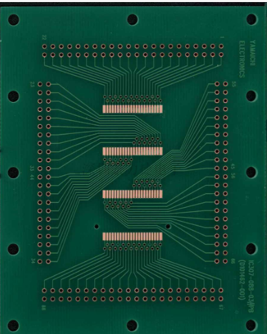
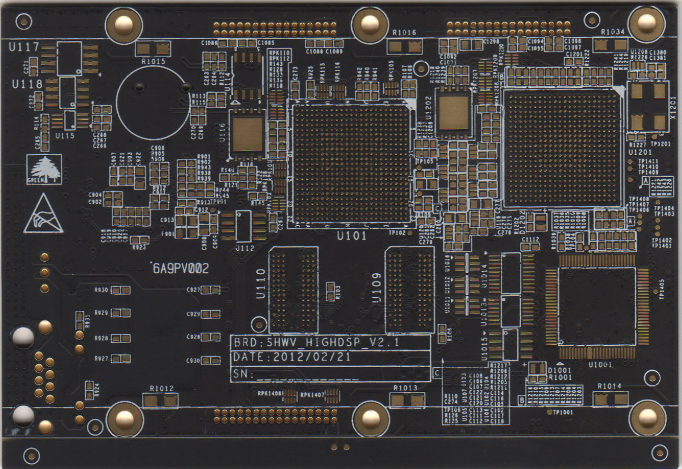
Printed circuit boards with blind buried and blind hole structures are generally completed by "sub-board" production methods, which means that they must be completed through multiple pressing, drilling, and hole plating, so precise positioning is very important of.
The high-precision printed circuit refers to the use of fine line width/spacing, micro holes, narrow ring width (or no ring width), and buried and blind holes to achieve high density.
High precision means that the result of "fine, small, narrow, and thin" will inevitably lead to high precision requirements. Take the line width as an example: O.20mm line width, if it is produced in accordance with the regulations, it is qualified to produce 0.16-0.24mm. The error is (O.20 soil 0.04) mm; and the line width of O.10 mm, the error is (0.10 ± O.02) mm, obviously the accuracy of the latter is doubled, and so on is not difficult to understand, Therefore, the high-precision requirements will not be discussed separately.

Buried, blind, and through-hole technology The combination of buried, blind, and through-hole technology is also an important way to increase the density of printed circuits. Generally, the buried and blind holes are all tiny holes. In addition to increasing the number of wiring on the board, the buried and blind holes are interconnected with the "nearest" inner layer, which greatly reduces the number of through holes formed, and the setting of the isolation disk will also be greatly reduced. Reduce, thereby increasing the number of effective wiring and inter-layer interconnection in the board, and improving the high density of interconnection.
The Problem of Coincidence Between Layers in the Manufacturing of Blind and Buried Multilayer Printed Circuit Boards
By adopting the pin front positioning system of ordinary multilayer printed board production, the graphic production of each layer of single chip is unified into a positioning system, which creates conditions for the realization of successful manufacturing.
For the ultra-thick single chip used this time, if the board thickness reaches 2 mm, a certain thickness layer can be milled at the location of the positioning hole, and it is also attributed to the processing of the four-slot positioning hole punching equipment of the front positioning system Ability.