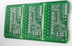
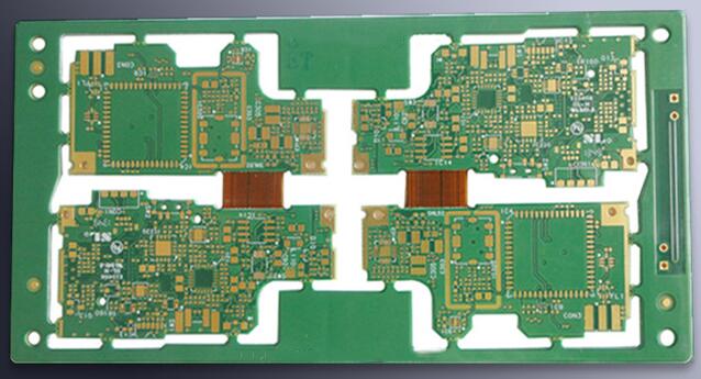
What are the PCB board design and wiring requirements?
What are the PCB board design and wiring requirements? Let's take a look at the following:
1. No cross circuit is allowed in the printed circuit. For possible crossover lines, it can be solved by "drilling" or "winding". In other words, let a certain lead pass through the gap under the pins of other resistors, capacitors, and transistors; or use jumpers to simplify the design to solve the cross-circuit problem.
2. Resistors, diodes, tubular capacitors and other components can be installed in two ways: "vertical" and "horizontal". Vertical refers to the installation and soldering of the component body perpendicular to the circuit board, and horizontal refers to the installation and soldering of the component body in parallel and close to the circuit board. Different mounting parts have different hole spacing on the printed circuit board.
3. The grounding point of the circuit of the same level should be as close as possible, and the power filter capacitor of the current level circuit should also be connected to the grounding point of the level. In particular, the grounding point of the base and emitter of the transistor of this level should not be too far away. The circuit using this "single point grounding method" is stable and not easy to self-excite.

4. The total ground wire must strictly follow the first-order principle of high frequency, intermediate frequency and low frequency, in the order of weak current to strong power. Especially the grounding wire arrangement requirements of the inverter head, regeneration head and FM head are more stringent. For high-frequency circuits such as FM heads, a large-area closed ground wire is usually used to ensure good shielding.
5. High-current leads (common ground, power amplifier power leads, etc.) should be as wide as possible to reduce wiring resistance and voltage, and reduce self-excitation caused by parasitic coupling.
6. High-impedance traces should be as short as possible, and low-impedance traces should be as long as possible. High-impedance traces are prone to ripple and absorb signals, which can cause circuit instability. The base track of the emitter follower and the ground of the two channels of the recorder must be separated, and each channel forms a way until the end of the function, such as bidirectional grounding.
The above are some requirements for PCB board design and wiring, I hope it will be helpful to you.
iPCB is a high-tech manufacturing enterprise focusing on the development and production of high-precision PCBs. iPCB is happy to be your business partner. Our business goal is to become the most professional prototyping PCB manufacturer in the world. Mainly focus onmicrowave high frequency PCB, high frequency mixed pressure, ultra-high multi-layer IC testing, from 1+ to 6+ HDI, Anylayer HDI, IC Substrate, IC test board, rigid flexible PCB, ordinary multi-layer FR4 PCB, etc. Products are widely used in industry 4.0, communications, industrial control, digital, power, computers, automobiles, medical, aerospace, instrumentation, Internet of Things and other fields.