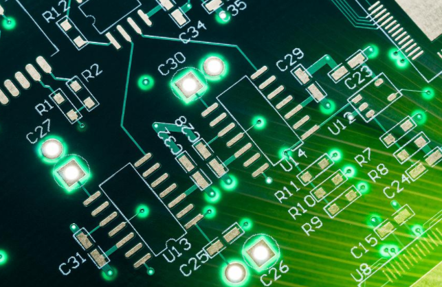
What knowledge should be mastered for PCB board wiring?
PCB wiring is to lay out printed wires according to the PCB circuit schematic diagram, wire table, and required wire width and spacing. So, what knowledge should be mastered for PCB board wiring?
1. The wiring should be as simple as possible on the premise of meeting the requirements. The order of selecting the wiring method is single layer-double layer-multilayer.
2. Ground wire shielding should be laid next to the input line of the analog circuit; the wiring of the same layer should be evenly distributed; the conductive area of each layer should be relatively balanced.
3. When changing the direction of the signal line, it should be obliquely or smoothly transitioned to avoid electric field concentration, signal reflection and additional impedance.

4. The wiring of the digital circuit and the analog circuit should be separated to avoid mutual interference; the signal lines of different frequencies should be separated by a grounding wire to avoid crosstalk. For the convenience of testing, necessary breakpoints and test points should be set in the design.
5. When the circuit components are grounded and connected to the power supply, the wiring should be as short as possible and as close as possible to reduce internal resistance.
6. The upper and lower layers should be perpendicular to each other to reduce coupling, and the upper and lower layers should not be aligned or parallel.
7. Multiple I/O lines of high-speed circuits, and I/O lines of circuits such as differential amplifiers and balanced amplifiers should be of equal length to avoid unnecessary delay or phase shift.
8. When the PCB pad is connected to a large area conductive area, a thin wire with a length of not less than 0.5m should be used for thermal isolation, and the width of the thin wire should not be less than 0.13mm.
9. The wire closest to the edge of the SMB should be more than 5mm away from the edge of the SMB. The ground wire can be close to the edge of the SMB when necessary.
10. The public power and ground wires on the double-sided SMB should be routed as close to the edge of the SMB as possible, and distributed on both sides of the SMB. The multi-layer SMB can be provided with a power layer and a ground layer on the inner layer, which are connected to the power and ground wires of each layer through metallized holes. The large-area wires, power wires and ground wires of the inner layer should be designed into a mesh.
The above is the knowledge that engineers need to master the wiring of PCB boards for you in detail, do you understand it? iPCB is a high-tech manufacturing enterprise focusing on the development and production of high-precision PCBs. iPCB is happy to be your business partner. Our business goal is to become the most professional prototyping PCB manufacturer in the world. Mainly focus on microwave high frequency PCB, high frequency mixed pressure, ultra-high multi-layer IC testing, from 1+ to 6+ HDI, Anylayer HDI, IC Substrate, IC test board, rigid flexible PCB, ordinary multi-layer FR4 PCB, etc. Products are widely used in industry 4.0, communications, industrial control, digital, power, computers, automobiles, medical, aerospace, instrumentation, Internet of Things and other fields.