What are the precautions for the layout of PCB circuit board components?
In the PCB manufacturing process, the layout of components is an important part. Improper placement will cause circuit compatibility problems and signal integrity problems, which will lead to the failure of PCB design. So, what are the precautions for PCB circuit board component layout?
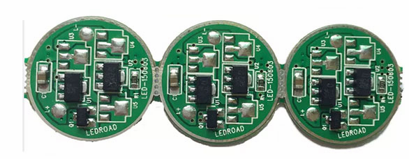
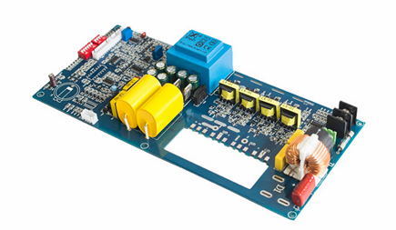
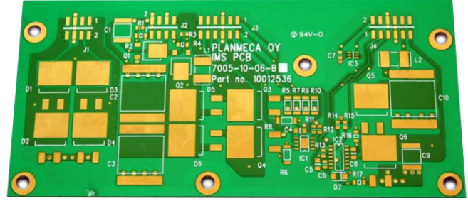
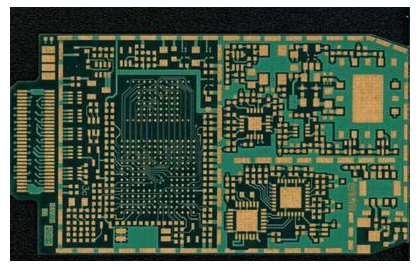
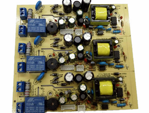
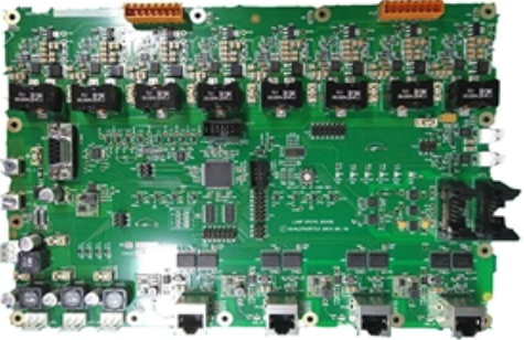
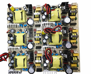
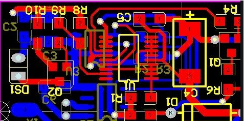
PCB circuit board component layout
1. Under the premise of ensuring the electrical performance, the components should be placed on the grid and parallel or perpendicular to each other, so as to be neat and beautiful. Under normal circumstances, they are not allowed to overlap; the components should be arranged compactly and distributed evenly on the entire layout., The density is consistent.
2. Under normal circumstances, all components should be arranged on the same surface; only when the top components are too dense, can some devices with limited height and low heat generation, such as chip resistors, chip capacitors, chip ICs, etc. On the lower floor.
3. Take the core components of each functional unit as the center and lay out around it; minimize and shorten the leads and connections between the components.

4. The components are generally not less than 2mm away from the edge of the PCB.
5. The minimum distance between different components should be above 1mm.
6. For circuits operating at high frequencies, the distribution parameters between components should be considered.
7. The location of special components needs to be carefully analyzed. First determine the size of the PCB, and then determine the placement of special components; finally, according to the functional unit, layout all the components of the circuit.
8. Inspection of component layout:
(1) Whether the size meets the requirements of the drawings.
(2) Whether there are conflicts at all levels. For example, whether the components, the frame, and the level of private printing are reasonable.
(3) Whether the layout of the components is balanced and neatly arranged, and whether they have all been laid out.
(4) Whether the heat dissipation is good.
(5) Whether the distance between thermal components and heating components is reasonable.
(6) Whether the line interference problem needs to be considered.
(7) Whether the commonly used components are convenient to use.
The above are some precautions for the layout of PCB circuit board components, I hope to help you all.