The interconnection of the circuit board system includes three types of interconnection between the chip to the circuit board, the interconnection within the PCB board, and the PCB and external devices. In RF design, one of the main problems faced by the engineering design of electromagnetic characteristics at the interconnection point. This article introduces the various techniques of the above three types of interconnection design, including device installation methods, wiring isolation and measures to reduce lead inductance, etc. Wait.
There are currently signs that the frequency of printed circuit board design is getting higher and higher. As the data rate continues to increase, the bandwidth required for data transmission also promotes the upper limit of the signal frequency to 1GHz or even higher. Although this kind of high-frequency signal technology is far beyond the range of millimeter wave technology (30GHz), it does also involve RF and low-end microwave technology.
The RF engineering design method must be able to deal with the stronger electromagnetic field effects that are usually generated at higher frequency bands. These electromagnetic fields can induce signals on adjacent signal lines or PCB lines, resulting in unpleasant crosstalk (interference and total noise), and can impair system performance. The return loss is mainly caused by impedance mismatch, and the influence on the signal is the same as the influence caused by additive noise and interference.
High return loss has two negative effects: 1. The signal reflected back to the signal source will increase the system noise, making it more difficult for the receiver to distinguish the noise from the signal; 2. Any reflected signal will basically degrade the signal quality because of the input signal The shape has changed.
Although the digital system only processes 1 and 0 signals and has very good fault tolerance, the harmonics generated when the high-speed pulse rises will cause the higher the frequency, the weaker the signal. Although the forward error correction technology can eliminate some negative effects, part of the system bandwidth is used to transmit redundant data, which leads to a decrease in system performance. A better solution is to let RF effects help rather than detract from signal integrity. It is recommended that the total return loss of the digital system at the highest frequency (usually the poor data point) is -25dB, which is equivalent to a VSWR of 1.1.

The goal of PCB design is smaller, faster and lower cost. For RFPCB, high-speed signals sometimes limit the miniaturization of PCB design. At present, the main method to solve the crosstalk problem is to manage the ground plane, to space between wiring and to reduce the lead inductance (studcapacitance). The main method to reduce the return loss is impedance matching. This method includes effective management of insulating materials and isolation of active signal lines and ground lines, especially between signal lines that have transitioned states and ground.
Since the interconnection point is the weakest link in the circuit chain, in the RF design, the electromagnetic properties at the interconnection point are the main problems faced by the engineering design. Each interconnection point must be investigated and the existing problems must be solved. The interconnection of the circuit board system includes three types of interconnection: the chip to the circuit board, the interconnection within the PCB board, and the signal input/output between the PCB and external devices.
The interconnection between the chip and the PCB board
Pentium IV and high-speed chips containing a large number of input/output interconnection points are already available. As far as the chip itself is concerned, its performance is reliable, and the processing rate has been able to reach 1GHz. At the recent GHz Interconnect Symposium, the most exciting thing is that the methods for dealing with the ever-increasing number and frequency of I/O have been widely known. The main problem of chip and PCB interconnection is too high interconnection density will cause the basic structure of PCB material to become a factor limiting the growth of interconnection density. An innovative solution was proposed at the meeting, that is, the use of a local wireless transmitter inside the chip to transmit data to the adjacent circuit board.
Regardless of whether this scheme is effective or not, the participants are very clear: In terms of high-frequency applications, IC design technology is far ahead of PCB design technology.
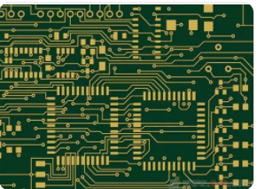
The skills and methods for high frequency PCB design with the interconnection in the PCB board are as follows:
1. The corner of the transmission line should be 45° to reduce the return loss;
2. High-performance insulated circuit boards with insulation constant values strictly controlled according to the level shall be used. This method is conducive to effective management of the electromagnetic field between the insulating material and the adjacent wiring.
3. To improve the PCB design specifications related to high-precision etching. It is necessary to consider that the total error of the specified line width is +/-0.0007 inches, the undercut and cross-section of the wiring shape should be managed, and the plating conditions of the wiring side wall should be specified. The overall management of wiring (wire) geometry and coating surface is very important to solve the skin effect problem related to microwave frequency and realize these specifications.
4. The protruding leads have tap inductance, so avoid using components with leads. In high frequency environments, it is best to use surface mount components.
5. For signal vias, avoid using a via processing (pth) process on sensitive boards, because this process will cause lead inductance at the vias, such as a via on a 20-layer board for connection 1 Up to 3 layers, the lead inductance can affect 4 to 19 layers.
6. To provide abundant grounding layers, use molded holes to connect these grounding layers to prevent the 3D electromagnetic field from affecting the circuit board.
7. To choose electroless nickel plating or immersion gold plating process, do not use HASL method for electroplating. This kind of electroplated surface can provide better skin effect for high frequency current. In addition, this highly solderable coating requires fewer leads, which helps reduce environmental pollution.
8. The solder mask can prevent the flow of solder paste. However, due to the uncertainty of the thickness and the unknown of the insulation performance, the entire surface of the board is covered with solder mask material, which will cause a large change in the electromagnetic energy in the microstrip design. Generally, a solder dam is used as the solder mask.
If you are not familiar with these methods, you can consult with experienced design engineers who have been engaged in military microwave circuit board design. You can also discuss with them the price range you can afford. For example, the copper-backed coplanar microstrip design is more economical than the stripline design. You can discuss this with them for better construction. Good engineers may not be accustomed to considering cost issues, but their suggestions are also quite helpful. Now try to train young engineers who are unfamiliar with RF effects and lack experience in handling RF effects. This will be a long-term job. In addition, other solutions can also be adopted, such as improving the computer type to enable it to handle RF effects.
It can now be considered that we have solved all the signal management problems on the board and the interconnection of individual discrete components. So how to solve the problem of signal input/output from the circuit board to the wires connected to the remote device? Trompeter Electronics, an innovator of coaxial cable technology, is working to solve this problem and has made some important progress. Also, take a look at the electromagnetic field given. In this case, we manage the conversion from microstrip to coaxial cable. In the coaxial cable, the ground layer is interwoven ring-shaped and evenly spaced. In microstrip, the ground plane is below the active line.