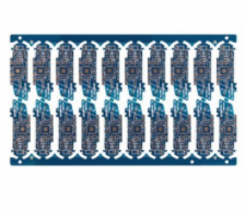
Circuit board production plant: PROTEL technology
Circuit board manufacturer: PROTEL technology 1. The schematic diagram is often incorrect:
(1) The ERC report states that the pin is not connected to a signal:
A. I/O attributes were defined for the pins when the package was created;
B. When creating a component or placing a component, the different grid attributes are corrected, and the pins and wires are not connected;
C. When creating the component, the pin direction is reversed, and the non-pin name end must be threaded.
(2) The component went outside the drawing boundary: no component was created in the core of the component library chart paper.
(3) The project file network table created can only be imported into PCB partly: when generating netlist, it is not selected as global.
(4) When using self-created multi-part components, be sure not to use annotate.
2. The PCB board is not correct in the middle:
(1) Online report conforms to the fashion report statement NODE did not find:
A. The components in the schematic diagram use packages that are not in the PCB library;
B. The components in the schematic diagram use packages with different names in the PCB library;
C. The components in the schematic diagram use packages with different pin numbers in the PCB library. If there is a tube with three electrodes: the pin number in sch is e, b, c, and the pin number in PCB is 1, 2, 3.

(2) It is always impossible to print onto one page when printing:
A. Not at the origin when creating the PCB library;
B. The component has been moved and rotated many times, and there are hidden characters outside the boundary of the PCB board. Select the characters that reveal all the masks, change from large to small PCB, and then move the characters to the boundary.
(3) The DRC report states that the network is divided into several parts:
express that this network is not connected, look at the report statement file, and use the selected CONNECTED COPPER search.
Additionally remind friends to try their best to use WIN2000 to reduce the chance of blue screen; export the file several times to make a new DDB file, which reduces the file size and the chance of protel deadlock. If you make more complicated presets, try your best not to use semi-automatic routing.
In the PCB preset, wiring is the key step to complete the product preset. It can be said that the preparation and office in front of it are all done for it. In the entire PCB, the wiring preset process is the most framed, the technique is the most detailed and the office The largest amount. PCB wiring includes single-sided wiring, double-sided wiring and multilayer wiring. There are also two types of wiring: semi-automatic wiring and interactive wiring. Before semi-automatic wiring, you can use interactive to pre-wire the wires with strict requirements. The edges of the input end and the output end should be prevented from being adjacent to parallel to avoid reflection interference. When it is indispensable, the ground wire should be added for isolation, and the wiring of two adjacent layers should be vertical to each other, and parasitic coupling can easily occur in parallel.
The layout rate of semi-automatic routing depends on a satisfactory layout. The routing rules can be pre-set, covering the number of buckling turns of the trace, the number of vias, the number of steps, etc. Ordinarily implement the longitude of the test-based cloth first, quickly connect the short wires, and then perform the field-based wiring that is not easy to explore, first implement the whole situation of the cross wires to be clothed: the wiring route of the mind ~ is optimized, and it can break the cloth according to the demand. String. And try to re-wiring to improve the overall effect.
For the high density PCB presets up to now, it has been felt that through holes are not suitable. It consumes a lot of precious wiring channels. In order to solve this contradiction, blind hole and buried hole technology has been revealed, which is more than complete. In addition to the effect of vias, it also saves a lot of wiring channels to make the wiring process more convenient, smoother, and more complete. The PCB board preset process is a complex and simple process. If you want to master it well, It is also necessary for the majority of electronic engineering personnel who have assumed positions to experience and comprehend by themselves, and the ability to obtain the true meaning of it.
1 Disposal of power supply and ground wire
Even if the wiring in the entire PCB board is completed well, the interference caused by the improper thinking of the power supply and the ground wire will degrade the performance of the product, and sometimes even affect the success rate of the product. Therefore, the wiring of electricity and ground wires should be taken seriously, and the noise interference generated by the electricity and ground wires should be reduced to the limit to ensure the quality of the products.
Everyone who works in the pre-designed project of electronic products knows the origin of the noise between the blank land line and the power line. Now I only describe the reduced noise control:
A household name is to add decoupling capacitors between the power supply and ground. 7 X2 B3 K) Y/ ?" e( A1 F/ t# Y4 x, n try to widen the width of the power and ground wires, preferably the ground wire is wider than the power wire, their relationship is: ground wire>power wire> Signal line, the general signal line width is: 0.2~0.3mm, the smallest width can reach 0.05~0.07mm, the power line is 1.2~2.5 mm For the PCB of the digital circuit, a wide ground wire can be used to form a loop, that is, a ground Use the net (the ground that imitates the circuit cannot be used in this way)
Use large and small copper layers on the surface of the object as the ground wire, and connect the unused places on the printed circuit board as the ground wire. Or it can be made into a multilayer board, and the power supply and ground wires occupy one layer each.
2. Common ground handling of digital circuits and analog circuits
Nowadays, many PCBs are no longer purely one-function circuits (digital or analog circuits), but are composed of a mixture of digital circuits and analog circuits. Because of this, it is necessary to think about the problem of mutual interference between them when wiring, especially the noise interference on the ground wire.
The frequency of digital circuits is high, and the sensitivity of analog circuits is strong. For signal lines, high-frequency signal lines are as far away as possible from sensitive analog circuit components. For ground lines, the whole PCB has only one node to the outside world. Therefore, it is necessary to deal with the problem of digital and analog common ground in the PCB. In the board, the digital ground and the analog ground are actually separated. They are not connected to each other, but at the interface (such as plugs, etc.) between the PCB and the outside world. . There is a short connection between the digital land and the mimic land. Please note that there is only one connection point. There are also non-common grounds on the PCB, which is voted on by the system default.
3, the signal line is laid on the electric (ground) layer
In the multi-layer printed board wiring, because there are few lines left in the signal line layer that have not been laid out, adding more layers will cause cost and increase the output of a certain amount of office, and the cost will increase accordingly. In order to solve this Contradiction, you can think about the problem in the electrical (ground) layer upward wiring. The power layer should be used first to think about the problem, and the second is the ground layer. Because it is best to preserve the integrity of the formation.
4. Disposal of connecting legs in large and small conductors on large planes or surface of objects
In the grounding (electricity) of the size of the large plane or the surface of the object, the legs of the commonly used components are connected to them, and comprehensive thinking is implemented on the disposal requirements of the connected legs. In terms of electrical performance, the pads of the component legs and the copper Full surface connection is good, but there are some hidden dangers in the welding assembly of the components, such as: 1. The welding requires high-power heaters. 2. It is easy to cause false solder joints. Therefore, both electrical performance and process requirements are made into cross-patterned pads, which are called heat shields, commonly known as thermal pads. In this way, it can cause the initiation of virtuality due to the cross-section of the welding and the heat dissipation. The possibility of solder joints is greatly reduced. The handling of the power (ground) leg of the multilayer board is the same.