How to make a PCB board?
1. Draw the component library
2. Draw the schematic
3. Draw the package library
4. Import the netlist
5. Layout
6. Draw a line
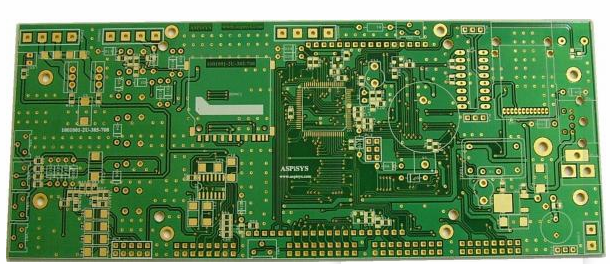
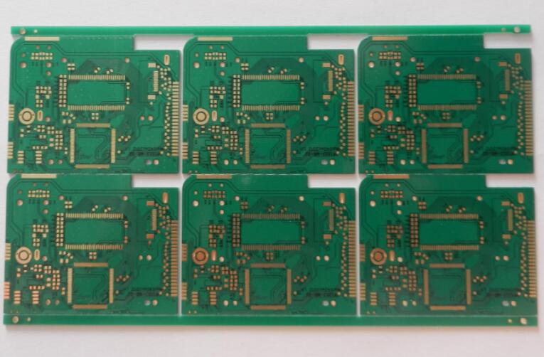
After finishing the PCB board finally
Generally, it must be made into a GERBER file and sent to the PCB manufacturer
The manufacturer’s steps are
1. Single panel process flow
Cutting edge grinding - drilling - outer layer graphics - (full plate gold plating) - etching - inspection - silk screen solder mask - (hot air leveling) - silk screen characters - shape processing - testing - inspection
2. Process flow of double-sided tin spraying board

Cutting edge grinding - drilling - heavy copper thickening - outer layer graphics - tin plating, etched tin removal - secondary drilling - inspection and inspection - silk screen solder mask - gold-plated plug - hot air leveling - silk screen characters - shape processing - Test - check
3. Double-sided nickel-gold plating process
Cutting edge grinding - drilling - heavy copper thickening - outer layer graphics - nickel plating, gold removal and etching - secondary drilling - inspection and inspection - silk screen solder mask - silk screen characters - shape processing - testing - inspection and inspection
4. Multi-layer board tin spraying process flow
Cutting and grinding - drilling positioning holes - inner layer graphics - inner layer etching - inspection and inspection - blackening - lamination - drilling - copper thickening - outer layer graphics - tin plating, etched tin removal - secondary drilling Hole - Inspection - Screen printing solder mask - Gold-plated plug - Hot air leveling - Silk screen characters - Shape processing - Test - Inspection
5. Process flow of nickel-gold plating on multilayer boards
Cutting and grinding - drilling positioning holes - inner layer graphics - inner layer etching - inspection and inspection - blackening - lamination - drilling - copper thickening - outer layer graphics - gold plating, film removal and etching - secondary drilling -Inspect -Silk screen solder mask -Silk screen characters -Shape processing -Test -Inspect
6. Process flow of multi-layer plate immersion nickel gold plate
Cutting and grinding - drilling positioning holes - inner layer graphics - inner layer etching - inspection and inspection - blackening - lamination - drilling - copper thickening - outer layer graphics - tin plating, etched tin removal - secondary drilling Hole-inspection-screen printing solder mask-electroless nickel gold-screen printing characters-shape processing-test-inspection
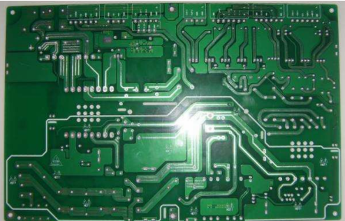
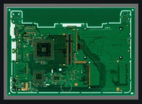
After the final PCB board is in hand
Manual soldering (the sample is still relatively small) or wave soldering (larger volume, basically all plug-ins) or soldering on SMT machine (larger volume, basically SMD components)
In the end, you will get a solid PCB that has been welded.
If you do it yourself, here is a video file: it can be engraved (the machine is expensive) or it can be corroded: (more commonly used)
Washing, exposure, corrosion, lamination, copper sinking, solder mask, silk screen, gong or V-CUT, inspection and measurement, delivery. This is simple, you need to choose a software to manufacture PCB, drawing, as for the software It’s dying, it’s easy to use 99se, and all the software is roughly the same. All components are deployed first.
After drawing the circuit, the network is generated and imported and then the PCB is produced. iPCB is a high-tech manufacturing enterprise focusing on the development and production of high-precision PCBs. iPCB is happy to be your business partner. Our business goal is to become the most professional prototyping PCB manufacturer in the world. Mainly focus on microwave high frequency PCB, high frequency mixed pressure, ultra-high multi-layer IC testing, from 1+ to 6+ HDI, Anylayer HDI, IC Substrate, IC test board, rigid flexible PCB, ordinary multi-layer FR4 PCB, etc. Products are widely used in industry 4.0, communications, industrial control, digital, power, computers, automobiles, medical, aerospace, instrumentation, Internet of Things and other fields.