The problem of solder joint peeling in SMT chip processing
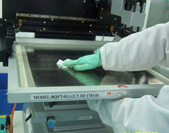
The phenomenon of solder joint peeling mostly occurs in the through-hole wave soldering process, but it has also occurred in the SMT reflow soldering process. The phenomenon is that there is a fault and peeling between the solder joint and the pad, as shown in Figure 1. The main reason for this kind of phenomenon is the large difference between the thermal expansion coefficient of lead-free alloys and the substrate, which causes too much stress in the peeled part of the solder joints to separate them, and the non-eutectic properties of some solder alloys are also One of the reasons for this phenomenon. Therefore, there are two main ways to deal with this PCB problem. One is to choose an appropriate solder alloy; the other is to control the cooling rate so that the solder joints solidify as soon as possible to form a strong bonding force. In addition to these methods, the magnitude of the stress can also be reduced by design, that is, the copper ring area of the through hole is reduced. A popular practice in Japan is to use SMD pad design, that is, to limit the area of the copper ring through the green solder mask. However, this approach has two undesirable aspects. One is that the slight peeling is not easy to see; the other is the formation of solder joints between the green oil and the interface of the SMD pad, which is not ideal from the point of view of life. of.

Some peeling phenomena appear on the solder joints, called cracks or tearing (Tearing). If this problem occurs on the wave through-hole solder joints, some suppliers in the industry consider it acceptable. Mainly because the key parts of the through hole are not in this place. But if it appears on the reflow solder joints, it should be considered a quality problem, unless the degree is very small (similar to wrinkles).
The presence of Bi has an impact on both reflow soldering and wave soldering processes, that is, solder joint peeling. Due to the migration characteristics of Bi atoms, only during and after the SMT soldering process, Bi atoms migrate to the surface and between the lead-free solder and the copper pad, resulting in a "secreted" undesirable thin layer, which is accompanied by the solder and PCB during use. The CTE mismatch between centralized procurement will cause vertical floating and cracking.
ipcb is a high-precision, high-quality PCB manufacturer, such as: isola 370hr PCB, high-frequency PCB, high-speed PCB, ic substrate, ic test board, impedance PCB, HDI PCB, Rigid-Flex PCB, buried blind PCB, advanced PCB, microwave PCB, telfon PCB and other ipcb are good at PCB manufacturing.