Although building an analog system looks like a return to the vacuum tube era, analog components and circuits will not disappear anytime soon, nor will the PCBs that support them. Purely analog circuit boards and mixed-signal PCBs are still important in many products and will continue to operate at a range of frequencies. Getting started with analog PCB design can be difficult where to start and what to consider, but we hope these guidelines will help you understand the steps you can take to ensure success.
Sometimes, it is better to consider analog PCBs and mixed-signal PCBs based on common design goals. Analog circuits and PCBs require special care, because the goal is usually to route signals and input them into components/circuits while ensuring low-noise operation. Then, the frequency range of the board's operation will determine some of the measures that need to be taken to ensure that the design operates as expected. In this guide, we will outline some standard analog PCB design and layout guidelines that you should consider. We will try to cover from low kHz frequencies to high millimeter wave frequencies.
Simulate PCB layer stacking
After the circuit is designed, the layer stack is the first stop of the design. The analog layer stack generally follows the same idea used to build a digital PCB stack. Pay attention to the following points:
Power supply and grounding: Plan to use a large number of grounds around the traces that transmit critical signals in the PCB layout, and plan the power rail routing accordingly. Newer designers may be accustomed to thinking about how to route important analog interconnects, but if you do this early, you can plan power and signal wiring accordingly.

High frequency power supply: If your analog board needs to transmit at high output power and high frequency, then you need to provide a very stable power supply, which may be high current. Plan to use a power plane instead of a rail on the inner layer, and place a ground plane on the adjacent layer.
Material selection: I think every designer wants to use low-loss PTFE-based laminates for each layer of the analog circuit board, but these expensive materials are not always necessary. If your operating frequency is not tens of GHz, and you only use short wiring, as long as you don't wire very long interconnects, you can use standard FR4 laminate. If you really need a low-loss laminate, please contact your manufacturer to learn how to use a hybrid PCB stack.
In mixed-signal PCBs, the recommendations for power and grounding are usually different, depending on whether your analog and digital parts require any direct wiring between them.
Mixed signal power supply
For mixed-signal power supplies, the power plane is usually divided into digital and analog parts, similar to the work done by digital power planes that work under different power supply voltages. These parts should be in the same layer and refer to the same ground plane on the adjacent layer. In addition, it is best to put the digital power rail only on the digital part of the circuit board, as is the analog power rail.
Schematic diagram of the layout of the analog and digital PWR/GND parts.
If the arrangement on the left side of the above figure must be used, separate digital and analog power planes should not be placed in two adjacent layers so that the planes overlap. If these two planes do overlap in adjacent layers, the two planes will have a high capacitance between the overlapping areas, thereby generating a strong displacement current. Since the potential between these two planes fluctuates during the switching process, this will result in cavity emission at radio frequency.
In addition, you should not create an interface between the digital and analog parts by wiring the gaps between the analog and digital parts. To understand why, check this article. The interface you need can be provided by the ADC, which may be built into your host controller or a dedicated IC.
Simulate component placement in PCB layout
As the PWR/GND plan above implies, only place analog components in the analog part, and only place digital components in the digital part. Unfortunately, we cannot cover all possible component placements, but we can briefly discuss some important components. The two most interesting components with some important layout guidelines are ADCs and amplifiers (including operational amplifiers).
Dealing with unused op amps
One component that must appear on the analog board is the operational amplifier. In many op amp ICs, some op amps will be idle. Any unused leads on the IC should be properly terminated. The unterminated (that is, floating) leads on the operational amplifier in the IC can generate noise and propagate into the working IC, thereby reducing signal integrity.
If you are using a single power rail, you should first short the output to the inverting input. This produces negative feedback and ensures that the output follows the input correctly. Next, connect a voltage divider with equal resistance to the non-inverting input and ground pins. This sets the input potential to the midpoint of the linear range. If you are using a split rail, you can simply short the output to the inverting input and ground the non-inverting input.
Problems with power amplifiers
At low frequencies, the amplifier will not be subject to any special restrictions that are not applicable to other PCBs. For power amplifiers operating at high frequencies, the situation is different, because the amplifier output may be unstable, which manifests as unexpected positive feedback. You can use some simulation to track the coupling back to the amplifier input, although these require a field solver that can interface directly with your PCB layout. Learn more about this interesting signal integrity issue involving RF power amplifiers.
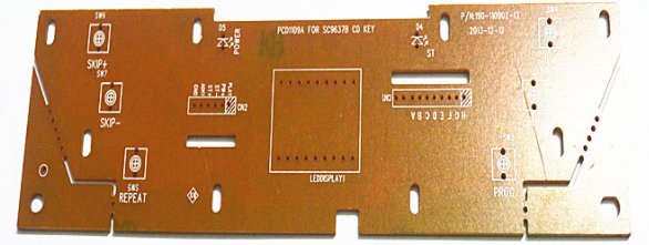
Where to place the ADC
ADC is where your analog signal connects with the digital world, so this part needs to be placed carefully because it will contain the digital part. Discrete ADCs are best placed roughly along the boundary between the digital and analog parts. In fact, this may be the only acceptable way to create an interface in a mixed-signal system with a separate ground plane, because the ground plane on the silicon chip can provide a reference plane for input/output signals. However, if you use a uniform ground plane, the placement of the ADC and the shielding provided by the ground plane will have more flexibility.
Analog PCB layout guide
The wiring in the analog PCB is to ensure that the analog signal sent along the interconnect will not be significantly distorted on the receiver side of the interconnect. When using an analog PCB, your net count is usually much less than in a digital PCB, so you can try some possible layouts as early as possible until you find a solvable floor plan. Here are some route guides:
Trace length: Generally speaking, try to keep the traces in the analog PCB as short and straight as possible. This is very important as the signal frequency increases. In addition to loss, we must also pay attention to the critical length of the signal.
Minimize the use of vias: Each via increases the loss of interconnect S-parameters, so it is best to minimize these losses and only perform necessary layer conversions when possible. For those through holes that still exist, they may generate strong radiation like an antenna
There are many issues to consider in analog PCB layout, but the right design tools and rule-driven design software will help you implement the guidelines needed to keep the analog system noise-free and ensure signal/power integrity.