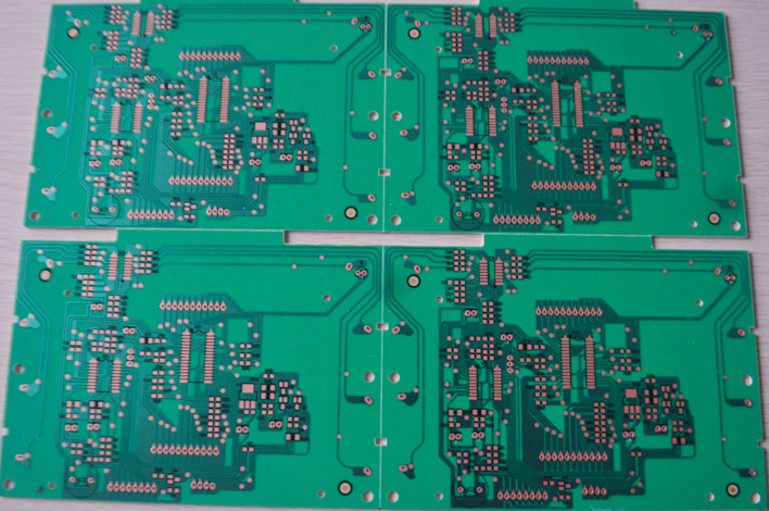
Engineers often face the challenge of shrinking system designs or packing additional functions in the same amount of printed circuit board(PCB) space. Due to the higher PCB density in smaller systems, designers may expect to increase the difficulty of board routing and board layout.
This article will explore analog signal chain products that are specifically developed to help engineers optimize board space without sacrificing the characteristics, cost, simplicity, or reliability of their systems. Its purpose is to help you understand how to use the advantages of these devices to develop compact, high-performance solutions for small spaces.
1. Operational amplifier and comparator: flexible packaging
In analog circuits, op amp amplifiers are popular because of their versatility. The operational amplifier makes a high-performance and high-stability amplifying circuit with few passive components. This is a good place to start the discussion, because the op amp combination has many performance levels and unique package options.

In the case of Texas Instruments, the op amplifier provides 16 different packages, including the smallest single-channel and four-channel packages in the industry, providing you with multiple options to help reduce the PCB area when you need it. Compared with competitors’ small devices, TI’s 0.8-0.8 mm leadless (X2SON) single-channel package is 13% smaller, and its 2.0-2.0 mm extra small QFN (X2QFN) package is 7% smaller.
Consider TLV9061 (single unit), TLV9062 (dual unit) and TLV9064 (four units) devices, which are low-voltage (1.8 to 5.5 V) op amplifiers with rail-to-rail input and output swing functions. TLV9061 is a compact single-channel op amp in its X2SON package, which is 8% smaller than competing devices. This 5.5 v op amp has a gain bandwidth of 10 mhz and a maximum offset voltage of 1.5 mv, providing a solution for low-voltage applications that require a small footprint and high capacitive load drive.
2. The smallest comparator in the industry
Similar to a standard op amp, the comparator has two input terminals, an output terminal and two power supply pins. The comparator gets its name because it compares the voltage applied to its input and sets the output voltage based on the input level.
One input is the main input signal VIN, and the other input is the reference signal VREF. These inputs can have DC and AC components.
The industry’s smallest comparator, TI’s TLV7081, is packaged in WCSP with a size of 0.7*0.7 mm, which is 4% smaller than competing products. The operating voltage of this comparator can be reduced to 1.7 V, so it is suitable for space-critical designs such as smartphones and other portable or battery-powered applications. The feature of TLV7081 is that the input voltage range is independent of the power supply voltage.
Therefore, the comparator can be directly connected to the power supply to be active, even if it is not powered.
3. The smallest lead current sense amplifier
As the demand for system intelligence and power efficiency continues to grow, better monitoring of critical system currents becomes more and more important. The most common method of measuring current is to detect the voltage drop across a shunt or current sense resistor.
TI's INA185 current-sense amplifier adopts a small-outline transistor (SOT)-563 package with a size of 1.6*1.6 mm (2.5 mm 2), which is 40% smaller than the closest similar lead package.
The device is designed for space-constrained applications and can sense the voltage drop across the current sense resistor at a common-mode voltage of -0.2 to +26 V, regardless of the supply voltage.
Using a current-sense amplifier with an integrated current-sense resistor can simplify resistor selection and PCB layout difficulties. INA185 integrates a matched resistive gain network in four fixed gain device options.
The matched resistance gain network in the amplifier can achieve a maximum gain error as low as 0.2%, which helps its performance within the range of temperature and process variations.
The INA185 has a gain error of 0.2% and a typical response time of 2 µs, which enables fast fault detection to prevent system damage.
4. Data converter: higher value per square millimeter
You can use small data converters to significantly reduce PCB footprint, increase channel density, and take advantage of higher integration of other components and functions.
For example, TI ADS7066 is a 16-bit, 8-channel successive approximation register (SAR) analog-to-digital converter (ADC), packaged in a package, can achieve the maximum channel density and save board space 54% less than competing devices.
ADS7066 has an integrated non-capacitance reference voltage source and a reference voltage buffer, by reducing the number of external components to help reduce the size of the overall solution. ADS7066 has a built-in offset calibration function, which can improve accuracy under a wide range of operating conditions.
The eight channels of ADS7066 can be configured as analog input, digital input or digital output respectively, thereby achieving a smaller system size and simplifying the circuit design of mixed signal feedback and digital control.
5 Conclusion
PCB factory packaging should include traditional ceramic and lead-containing options as well as advanced chip scale packaging-quad flat lead-free (QFN), chip chip scale packaging (WCSP) or die size ball grid array (DSBGA) using fine pitch wire bonds Hehe Flip Chip Interconnect, and provide SiP, module, stacked and embedded die formats.