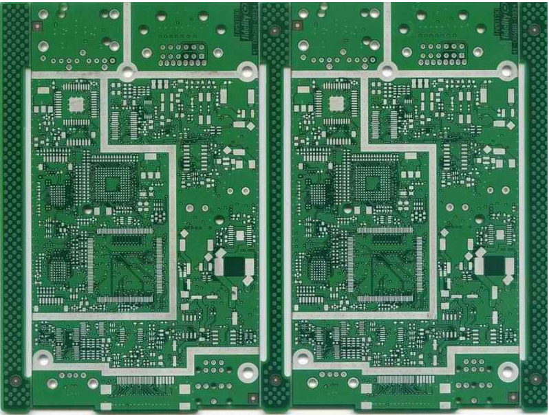
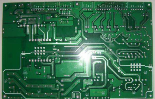
Nowadays, the updating speed of electronic products is extremely fast, which is simply overwhelming. Product design engineers are more inclined to choose AC/DC adapters that are easily available in the market, and install multiple sets of DC power supplies directly on the line of the system. On the board. Since the electromagnetic interference generated by the switching power supply will affect the normal operation of its electronic products, the correct layout of the power supply PCB becomes very important. Based on experience, the basic points of eight-point switching power supply PCB layout are summarized.
Here is a brief summary of what these eight points are.
Point 1. The capacitance of the bypass ceramic capacitor should not be too large, and its parasitic series inductance should be as small as possible. Multiple capacitors in parallel can improve the impedance characteristics of the capacitor;
Point 2, the parasitic parallel capacitance of the inductor should be as small as possible, the longer the distance between the inductor pin pads, the better;
Point 3. Avoid placing any power or signal traces on the ground;
Point 4, the area of the high-frequency loop should be as small as possible;
Point 5, the placement of vias should not destroy the path of high-frequency current on the ground;
Point 6. A small circuit on the system board requires different ground layers, and the ground layer of the small circuit is connected to the power ground layer through a single point;
Point 7, the drive circuit loop from the control chip to the upper and lower FETs should be as short as possible;
Point 8. The switching power supply power circuit and the control signal circuit components need to be connected to the ground plane of Xiaotong, and these two ground planes are generally connected through a single point.

The switching power supply contains high-frequency signals. Any printed line on the PCB board can function as an antenna. The length and width of the printed line will affect its impedance and inductance, thereby affecting the frequency response. Therefore, the placement of the grounding wire should be carefully considered in the layout. Mixing various groundings will cause unstable power supply operation.
The following points should be paid attention to in the ground wire design:
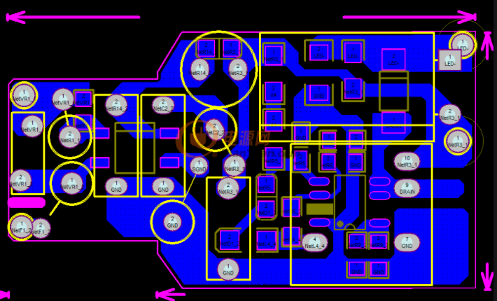
1. Correctly choose single-point grounding. Generally, the common end of the filter capacitor should be the only connection point for other grounding points to couple to the AC ground of high current. It should be connected to the grounding point of this level. The main consideration is that the current returning to the ground in each part of the circuit is changed. The impedance of the actual flowing line will cause the change of the ground potential of each part of the circuit and introduce interference. In this switching power supply, its wiring and the inductance between the devices have little influence, and the circulating current formed by the grounding circuit has a greater influence on the interference. Connected to the ground pin, the ground wires of several components of the output rectifier current loop are also connected to the ground pins of the corresponding filter capacitors, so that the power supply works more stably and is not easy to self-excite. When a single point is not available, share the ground Connect two diodes or a small resistor, in fact, it can be connected to a relatively concentrated piece of copper foil.
2. Thicken the grounding wire as much as possible. If the grounding wire is very thin, the ground potential will change with the change of the current, causing the timing signal level of the electronic equipment to be unstable and the anti-noise performance to deteriorate. Therefore, ensure that each large current grounding terminal Use printed lines as short and wide as possible, and widen the width of the power and ground lines as much as possible. The ground line should be wider than the power line. Their relationship is: ground line>power line>signal line. If possible, ground line The width should be greater than 3mm, and a large area copper layer can also be used as a ground wire. Connect the unused places on the printed circuit board as a ground wire. When performing global wiring, the following principles must also be followed:
(1). Wiring direction: From the welding surface, the arrangement direction of the components should be as consistent as possible with the schematic diagram. The wiring direction should be consistent with the wiring direction of the circuit diagram, because various parameters are usually required on the welding surface during the production process. Therefore, it is convenient for inspection, debugging and maintenance in production (Note: It refers to the premise of meeting the circuit performance and the requirements of the whole machine installation and panel layout).
(2). When designing the PCB wiring diagram, the wiring should not bend as much as possible, the line width on the printed arc should not be changed suddenly, the corner of the wire should be ≥90 degrees, and the line should be simple and clear.
(3). Cross circuits are not allowed in the printed circuit. For the lines that may cross, you can use "drilling" and "winding" to solve the problem. That is, let a lead "drill" through the gap under other resistors, capacitors, and triode pins, or "wind" from one end of a lead that may cross. In special circumstances, how complex the circuit is, it is also allowed to simplify the design. Use wires to bridge to solve the cross circuit problem. Due to the single-sided board, the in-line components are located on the top surface and the surface-mount devices are located on the bottom surface, so the in-line devices can overlap with the surface-mount devices during layout, but overlap of the pads should be avoided.
3. Input ground and output ground This switching power supply is a low-voltage DC-DC. If you want to feedback the output voltage back to the primary of the transformer, the circuits on both sides should have a common reference ground. Therefore, after laying copper on the ground wires on both sides, you must Connect together to form a common ground