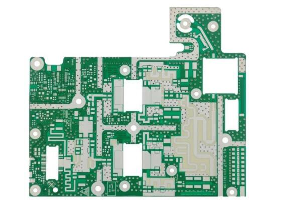
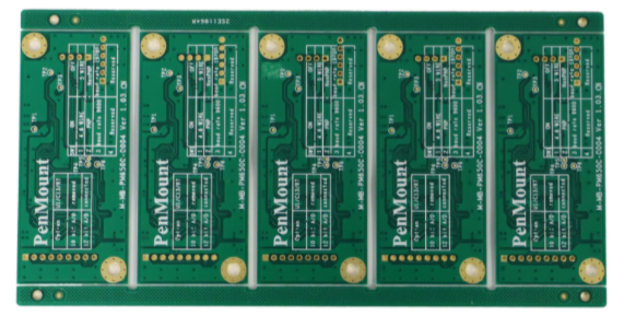
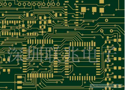
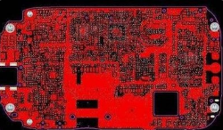
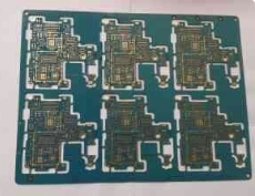
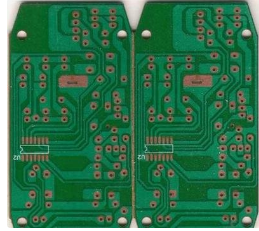
SMT patch refers to the abbreviation of a series of technological processes that are processed on the PCB basis . PCB (Printed Circuit Board) is a circuit board.
SMT is surface mount technology (Surface Mounted Technology) (abbreviation for Surface Mounted Technology), and it is currently the most popular technology and process in the electronics assembly industry. Electronic circuit surface mount technology (Surface Mount Technology, SMT), called surface mount or surface mount technology.
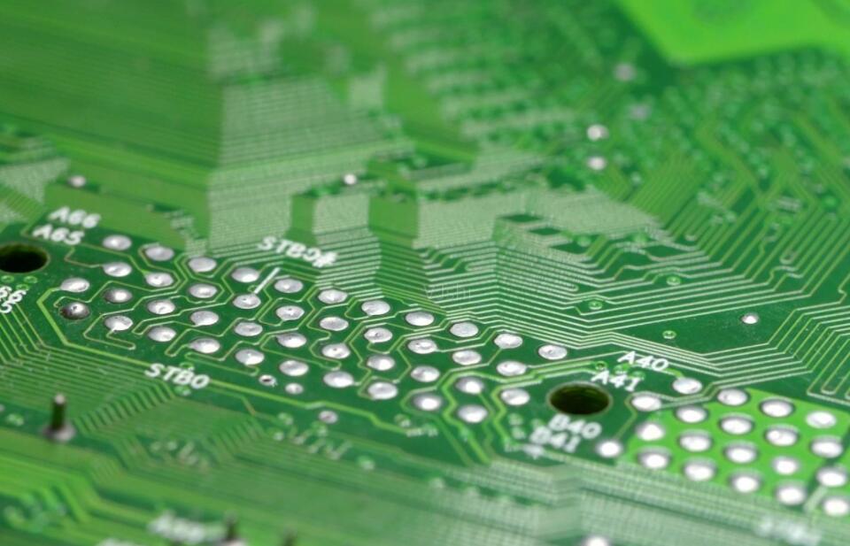
SMT is a kind of surface assembly components without leads or short leads (SMC/SMD for short, chip components in Chinese) mounted on the surface of PCB board or other substrates, and then soldered and assembled by reflow soldering or dip soldering. Circuit assembly technology. Click to learn more about SMT>>
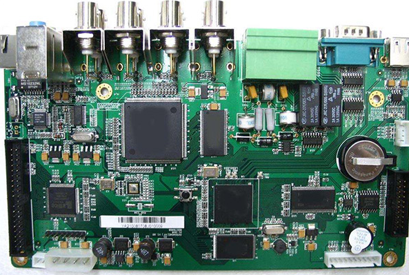
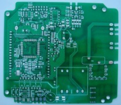
Under normal circumstances, the electronic products we use are designed by PCB plus various capacitors, resistors and other electronic components according to the designed circuit diagram, so all kinds of electrical appliances need a variety of smt chip processing techniques to process.
SMT basic process components: Solder paste printing --> parts placement --> reflow soldering -->AOI optical inspection --> maintenance --> sub-board.
Some people may ask why it is so complicated to connect an electronic component? This is actually closely related to the development of our electronic industry. Nowadays, electronic products are pursuing miniaturization, and the perforated plug-in components used in the past Can't zoom out anymore.

Electronic products have more complete functions, and the integrated circuits (ICs) used have no perforated components, especially large-scale, highly integrated ICs, and surface mount components have to be used. With mass production and production automation, PCB factories must produce high-quality products with low cost and high output to meet customer needs and strengthen market competitiveness, the development of electronic components, the development of integrated circuits (IC), and the diversified application of semiconductor materials. The revolution of electronic technology is imperative and chasing the international trend. It is conceivable that in the case of intel, amd and other international cpu and image processing device manufacturers whose production processes have advanced to more than 20 nanometers, the development of smt, such as surface assembly technology and technology, is also a situation that cannot be ignored.
The advantages of smt chip processing: high assembly density, small size and light weight of electronic products. The volume and weight of chip components are only about 1/10 of that of traditional plug-in components. Generally, after SMT is adopted, the volume of electronic products is reduced by 40%~60 %, the weight is reduced by 60%~80%. High reliability and strong anti-vibration ability. The defect rate of solder joints is low. Good high frequency characteristics. Reduce electromagnetic and radio frequency interference. It is easy to realize automation and improve production efficiency. Reduce costs by 30%~50%. Save materials, energy, equipment, manpower, time, etc.
It is precisely because of the complexity of the process flow of SMT chip processing that many smt chip processing plants have appeared. Thanks to the vigorous development of the electronics industry, smt chip processing has made an industry prosperous. Among them, Wanlong's lean smt processing is well-known in North China. Choose Wanlong to provide you with one-stop high-quality services.
SMT patch process
1. Single-sided assembly
Incoming inspection => silk screen solder paste (point patch glue) => patch => drying (curing) => reflow soldering => cleaning => inspection => repair
2. Double-sided assembly
A: Incoming inspection => PCB A-side silk-screen solder paste (dot SMD glue) => SMD PCB B-side silk-screen solder paste (dot SMD glue) => SMD => Drying => Reflow soldering ( It is best to only apply to side B => cleaning => inspection => repair).
B: Incoming inspection => PCB's A side silk screen solder paste (point patch glue) => SMD => Drying (curing) => A side reflow soldering => Cleaning => Turnover = PCB's B side point Patch glue => patch => curing => B surface wave soldering => cleaning => inspection => repair)
This process is suitable for reflow soldering on the A side of the PCB and wave soldering on the B side. In the SMD assembled on the B side of the PCB, this process should be used when there are only SOT or SOIC (28) pins or less.
3. Single-sided mixed packaging process:
Incoming inspection => PCB's A-side silkscreen solder paste (point patch glue) => SMD => drying (curing) => reflow soldering => cleaning => plug-in => wave soldering => cleaning => inspection = > Rework
4. Double-sided mixed packaging process:
A: Incoming inspection => PCB's B side point patch glue => SMD => curing => flipping => PCB's A side plug-in => wave soldering => cleaning => inspection => rework, paste first, then insert, Suitable for the situation where there are more SMD components than discrete components
B: Incoming inspection => PCB's A side plug-in (pin bend) => flip board => PCB's B side patch glue => patch => curing => flip board => wave soldering => cleaning => Inspection => Repair
Insert first, then paste, suitable for the situation where there are more separate components than SMD components
C: Incoming inspection => PCB A side silk screen solder paste => Patch => Drying => Reflow soldering => Plug-in, pin bending => Turnover => PCB side B point patch glue => Patch => curing => flipping => wave soldering => cleaning => inspection => rework A-side mixed assembly, B-side mounting.
D: Incoming inspection => PCB's B side spot patch glue => SMD => curing => flip board => PCB's A side silk screen solder paste => patch => A side reflow soldering => plug-in => Wave soldering on side B => cleaning => inspection => rework for mixed mounting on side A and mounting on side B. First paste on both sides of SMD, reflow soldering, then inserting, wave soldering E: Incoming inspection => PCB's B-side silk screen solder paste (point patch glue) => SMD => drying (curing) => reflow soldering = > Flip board => PCB's A-side silk screen solder paste => SMD => Drying = Reflow soldering 1 (partial soldering can be used) => Plug-in => Wave soldering 2 (If there are few components, manual soldering can be used) => Cleaning => Inspection => Rework A-side mounting and B-side mixed mounting.
5.PCB board double-sided assembly process
A: Incoming inspection, PCB A side silk screen solder paste (point patch glue), patch, drying (curing), A side reflow soldering, cleaning, flipping; PCB B side silk screen solder paste (point patch Glue), patch, drying, reflow soldering (preferably only for side B, cleaning, testing, repairing)
This process is suitable for picking when large SMDs such as PLCC are attached to both sides of the PCB.
B: Incoming inspection, PCB A side silk screen solder paste (dot patch adhesive), patch, drying (curing), A side reflow soldering, cleaning, flipping; PCB B side dot patch adhesive, patch, Curing, B-side wave soldering, cleaning, inspection, rework) This process is suitable for reflow on the A side of the PCB board.